
 My Inquiry
 My Account


onsemi NCP583XV30T2G
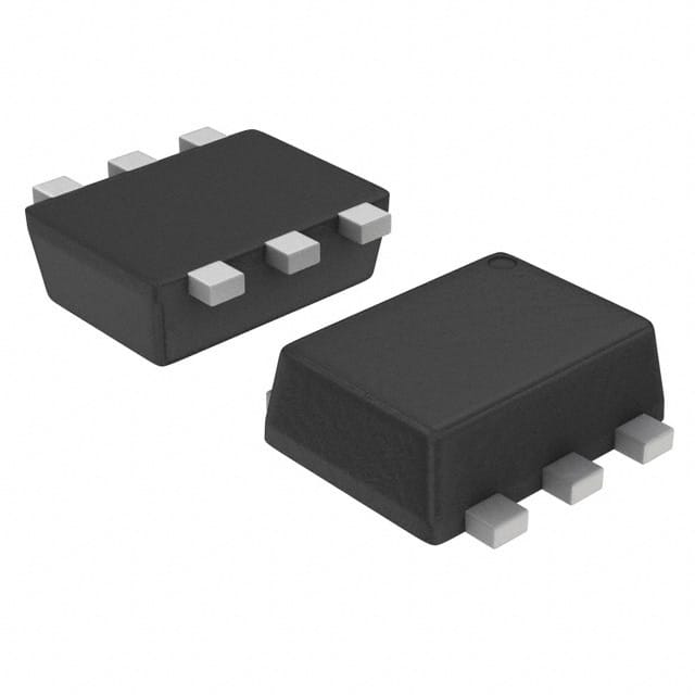
- Part No.:
- NCP583XV30T2G
- Manufacturer:
- onsemi
- Package:
- -
- Datasheet:
-
 NCP583XV30T2G.pdf
- Description:
- ANA LOW IQ 150MA LDO
- Quantity:
- Payment:

- Shipping:

Inventory:3,875
Please send an inquiry. Send us your inquiry, and we will respond immediately.
Product details
Overview
NCP583XV30T2G from onsemi is an ultra-low quiescent current (1.0 µA typical), 3.0 V fixed-output CMOS low-dropout regulator in SOT-563 package, delivering up to 150 mA output current with 2% output voltage accuracy and 250 mV dropout at full load - designed for battery-powered portable equipment requiring long runtime and stable voltage regulation.
For engineers reviewing the NCP583XV30T2G datasheet, pinout, applications, or equivalent options, key selection considerations include its 0.1 µA shutdown current, ±100 ppm/°C temperature coefficient, enable-controlled operation, and compatibility with 0.1 µF ceramic output capacitance.
Technical Context
The NCP583XV30T2G integrates a precision bandgap reference, error amplifier, and PMOS pass transistor in a CMOS architecture enabling ultra-low Iq without compromising transient response. Its enable input (CE) provides active-high logic control with 1.2 V to 6.0 V threshold range, supporting direct microcontroller interfacing.
It features foldback current limiting and thermal shutdown protection, operates across −40°C to +85°C ambient, and maintains regulation with input voltages from 1.7 V to 6.0 V - making it suitable for single-cell Li-ion, multi-cell alkaline, or regulated intermediate rail applications.
Key Specifications
| Parameter | Value and Actual Design Meaning |
|---|---|
| Output Voltage | Fixed 3.0 V ±2% - ensures stable power for 3.0 V logic, sensors, or RF modules without external feedback components. |
| Max Output Current | 150 mA - sufficient to power microcontrollers, BLE radios, or display drivers in compact portable systems. |
| Dropout Voltage | 250 mV at 150 mA - enables operation down to ~3.25 V input, extending usable battery life in single-cell Li-ion (3.0–4.2 V) applications. |
| Quiescent Current | 1.0 µA typical - minimizes standby power loss, critical for always-on IoT sensors or remote controls with multi-year battery life. |
| Shutdown Current | 0.1 µA typical - reduces system-level leakage when disabled via CE pin, preserving battery during deep sleep modes. |
| Line Regulation | 0.05%/V - maintains tight output stability despite input rail sag (e.g., battery discharge), reducing need for post-regulation filtering. |
| Temp Coefficient | ±100 ppm/°C - limits output drift to ±0.025 V over −40°C to +85°C, supporting precision analog front-ends without calibration. |
Pinout & Package
SOT−563 (Case 463A) - 6-pin, 1.6 mm × 1.2 mm × 0.6 mm surface-mount package with two ground pins (Pins 2 and 5) and one no-connect terminal (Pin 4), optimized for high-density PCB layouts and thermal performance (RJA = 200°C/W).
| Pin/Terminal | Circuit Role | Design Meaning |
|---|---|---|
| 1 | Vin | Input supply connection - accepts 1.7 V to 6.0 V; requires 1.0 µF ceramic decoupling to GND per datasheet recommendation. |
| 2 | GND | Power ground - primary return path for load current; must be connected to low-impedance ground plane. |
| 3 | Vout | Regulated 3.0 V output - drives load directly; requires 0.1 µF ceramic capacitor placed adjacent to pin for stability. |
| 4 | NC | No connect - electrically isolated; no PCB trace or solder mask opening required. |
| 5 | GND | Secondary ground - improves thermal dissipation and reduces ground bounce in high-transient-current scenarios. |
| 6 | CE | Active-high chip enable - pulls high (>1.2 V) to activate regulator; tied low (<0.3 V) to enter 0.1 µA shutdown mode. |
Key Features
| Feature | Design Value |
|---|---|
| Ultra-low dropout | 250 mV @ 150 mA enables use with depleting batteries while maintaining 3.0 V output - extends operational time in coin-cell or Li-ion systems. |
| 1.0 µA quiescent current | Reduces standby power to <3 nW per volt of input - critical for energy-harvesting or battery-backed real-time clocks. |
| 0.1 µA shutdown current | Allows complete system power gating without sacrificing fast wake-up (<10 µs typical turn-on time per datasheet curves). |
| ±2% output accuracy | Eliminates need for external trimming or calibration in cost-sensitive consumer electronics like wearables and remote controls. |
| Foldback current limit | Protects internal pass device during short-circuit events by reducing output current as Vout collapses - prevents thermal runaway. |
Applications
| Portable Medical Sensors | Wireless Remote Controls |
|---|---|
Use Scenario: Continuous glucose monitor (CGM) sensor node powered by CR2032 coin cell, operating 24/7 with periodic Bluetooth LE transmission. IC Role / Device Role / Timing Role: Primary 3.0 V power regulator for analog sensor front-end and BLE SoC, enabled only during measurement/transmit cycles. Use Value: 0.1 µA shutdown current extends battery life beyond 12 months; 250 mV dropout allows full utilization of coin cell's 2.0–3.0 V discharge curve. |
Use Scenario: IR-based universal remote using AAA alkaline cells, requiring low-power MCU wake-up on button press and RF transmission. IC Role / Device Role / Timing Role: Always-on LDO supplying real-time clock and wake-up circuitry; CE pin controlled by mechanical switch debounced via RC network. Use Value: 1.0 µA Iq ensures <1% annual self-discharge; ±2% output tolerance guarantees reliable MCU brown-out detection at 3.0 V threshold. |
| Industrial Handheld Scanners | Smart Home Motion Sensors |
Use Scenario: Rugged barcode scanner with laser diode, imager, and Bluetooth interface, powered by dual AA cells in series (2.4–3.2 V). IC Role / Device Role / Timing Role: Post-regulator stabilizing noisy switched-mode supply rail to clean 3.0 V for image sensor and decoder ASIC. Use Value: 0.05%/V line regulation rejects ripple from upstream DC-DC converter; 200°C/W thermal resistance supports continuous scanning without derating. |
Use Scenario: PIR-based occupancy sensor with Zigbee radio, operating on two AA cells in series, transmitting status every 5 minutes. IC Role / Device Role / Timing Role: Main power source for ultra-low-power MCU, PIR signal conditioner, and RF transceiver - enabled only during sensing/reporting windows. Use Value: ±100 ppm/°C tempco ensures consistent ADC reference across −10°C to +50°C ambient; NC pin simplifies layout in space-constrained enclosure. |
Equivalent & Alternatives
The following parts are listed as comparable options for similar LDO regulator applications.
| Alternative Part | Technical Difference | Application Difference | Selection Advice |
|---|---|---|---|
| MCP1700T-3002E/TT | 1.6 µA Iq, 600 mV dropout @ 250 mA, SOT-23-5 package | Higher dropout limits usable input range; larger footprint than SOT-563 | Prefer when higher output current (250 mA) is needed and board space permits larger package. |
| Torex XC6206P302MR-G | 1.0 µA Iq, 200 mV dropout @ 100 mA, SOT-25 package | Lower max current (100 mA); no dedicated CE pin - uses VIN-controlled enable | Prefer when strict 100 mA limit is acceptable and simplified enable logic (no separate CE trace) is desired. |
Compared with MCP1700T-3002E/TT and XC6206P302MR-G, the NCP583XV30T2G offers the lowest combination of dropout (250 mV @ 150 mA) and package density (SOT-563), while retaining independent CE control - making it optimal for space- and battery-life-constrained portable designs requiring 150 mA at 3.0 V.
Availability
NCP583XV30T2G is available at Aetrix Electronics and suitable for portable medical sensors, wireless remote controls, industrial handheld scanners, and smart home motion sensors requiring stable component supply, Pb-free compliance, and long-term manufacturability.
Supply support for NCP583XV30T2G includes scheduled delivery planning, volume procurement assistance, BOM continuity management, traceable sourcing, and lifecycle availability coordination for OEM customers, industrial embedded developers, connected-device designers, and electronics production programs.
Manufacturer
onsemi (formerly ON Semiconductor) is a global semiconductor supplier focused on energy-efficient electronics, delivering silicon solutions for automotive, industrial, cloud, and intelligent power systems.
The NCP583 series belongs to onsemi's ultra-low-Iq LDO portfolio, engineered specifically for battery-powered portable devices where extended runtime, small form factor, and precision regulation are critical design requirements.
FAQ
What is the maximum input voltage rating for the NCP583XV30T2G?
The NCP583XV30T2G has a maximum input voltage rating of 6.0 V under normal operating conditions, as specified in the Electrical Characteristics table. Absolute maximum ratings allow up to 6.5 V on Vin and CE pins, but sustained operation above 6.0 V may impact reliability and is not recommended for production designs using the NCP583XV30T2G.
Does the NCP583XV30T2G require an external capacitor on the output pin?
Yes, the NCP583XV30T2G requires a 0.1 µF ceramic capacitor on the Vout pin for stability, as confirmed in the Application Information section. A 1.0 µF ceramic capacitor is recommended on Vin, but the output capacitor is mandatory - omitting it risks oscillation or poor transient response in the NCP583XV30T2G.
Is the NCP583XV30T2G pin-compatible with other variants in the NCP583 family?
No - the NCP583XV30T2G uses the SOT-563 package (6-pin), while SC-82AB variants (e.g., NCP583SQ30T1G) use a 4-pin package. Pin count, pinout, and package dimensions differ; therefore, the NCP583XV30T2G is not pin-compatible with SQ-suffix parts, and PCB layout changes are required when substituting.
What is the typical enable threshold voltage for the CE pin of the NCP583XV30T2G?
The NCP583XV30T2G CE pin has a typical high-threshold voltage of 1.2 V and low-threshold of 0.3 V, as defined in the Electrical Characteristics table. This allows direct interfacing with 1.8 V or 3.3 V GPIOs without level-shifting - the NCP583XV30T2G turns on reliably when CE ≥1.2 V and shuts down fully when CE ≤0.3 V.
How does the NCP583XV30T2G handle thermal overload conditions?
The NCP583XV30T2G incorporates thermal shutdown protection that disables the output when junction temperature exceeds approximately 125°C. Recovery is automatic once temperature falls below the hysteresis threshold. This safeguard prevents permanent damage during sustained overload or poor PCB heat sinking - a core safety feature built into the NCP583XV30T2G.
NCP583XV30T2G Specifications
- Product attributes
- Attribute value
- Manufacturer:
- onsemi
- Series:
- *
- Package/Case:
- -
- Packaging:
- Tape & Reel (TR)
- Product Status:
- Obsolete
- Output Configuration:
- -
- Output Type:
- -
- Number of Regulators:
- -
- Voltage - Input (Max):
- -
- Voltage - Output (Min/Fixed):
- -
- Voltage - Output (Max):
- -
- Voltage Dropout (Max):
- -
- Current - Output:
- -
- Current - Quiescent (Iq):
- -
- Current - Supply (Max):
- -
- PSRR:
- -
- Control Features:
- -
- Protection Features:
- -
- Operating Temperature:
- -
- Grade:
- -
- Qualification:
- -
- Mounting Type:
- -
- Supplier Device Package:
- -
NCP583XV30T2G FAQ
1.How can I place an order for NCP583XV30T2G through Aetrix?
Please submit a Request for Quotation (RFQ) for NCP583XV30T2G on Aetrix. Our sales agent will provide a competitive quotation and guide you through the order confirmation once you accept the terms.
2.Are the price and stock information for NCP583XV30T2G reliable?
The price and inventory of NCP583XV30T2G are updated periodically and may fluctuate due to market conditions. Stock and pricing data are typically refreshed every 24 hours. Quotation validity for NCP583XV30T2G is usually 5 days.
3.What payment methods are accepted for NCP583XV30T2G?
We accept Wire Transfer, PayPal, Credit Card, Western Union, MoneyGram, and Escrow for NCP583XV30T2G transactions.
Note: Certain payment methods may incur a processing fee.
4.How is shipping managed for NCP583XV30T2G?
NCP583XV30T2G orders can be shipped via leading logistics carriers, including DHL, UPS, FedEx, TNT, or Registered Mail.
Once your NCP583XV30T2G order is processed, you will receive an email with the shipment details and tracking number.
Note: Tracking information may take up to 24 hours to appear. Express delivery typically takes 3–5 business days.
5.How can I obtain technical support or documentation for NCP583XV30T2G?
For technical support, including NCP583XV30T2G datasheets, pinout diagrams, or application guidance, please contact our engineering support team. They can provide detailed documentation and assistance for your NCP583XV30T2G requirements.
6.How does Aetrix verify that NCP583XV30T2G is sourced from the original manufacturer or authorized distributors?
All NCP583XV30T2G products on Aetrix are procured from qualified distributors and authorized channels. Our dedicated quality assurance team conducts strict verification, including traceability checks and, if necessary, third-party testing. This ensures that NCP583XV30T2G meets industry standards.
7.What is the process for return or replacement of NCP583XV30T2G?
All NCP583XV30T2G units undergo pre-shipment inspection (PSI). If there is an issue with NCP583XV30T2G, returns or replacements are accepted under the following conditions:
1.Quantity discrepancies, incorrect items, or visible external defects (such as breakage or corrosion), acknowledged by Aetrix.
2.The issue is reported within 90 days of delivery.
3.The NCP583XV30T2G part is unused and in its original packaging.
Return procedure for NCP583XV30T2G:
1.Submit a request within 90 days.
2.Obtain a Return Material Authorization (RMA) from Aetrix.
NCP583XV30T2G Tags

-
MIC5504-1.8YM5-TR
Microchip Technology
-
MIC5504-3.3YM5-TR
Microchip Technology

-
MIC5365-3.0YC5-TR
Microchip Technology
-
MIC5365-1.8YC5-TR
Microchip Technology
-
MIC5365-2.5YC5-TR
Microchip Technology
-
MIC5365-3.3YC5-TR
Microchip Technology

-
MIC5365-3.3YD5-TR
Microchip Technology

-
MIC5317-3.3YM5-TR
Microchip Technology

-
TLV1117LV33DCYR
Texas Instruments

-
MIC5317-3.3YMT-TZ
Microchip Technology

-
MIC5528-3.3YMT-TR
Microchip Technology

-
TLV75801PDRVR
Texas Instruments
Tech Hub

Counterfeit components can hide behind convincing markings and passing basic function tests. This engineering reference covers source traceability, external inspection, X-ray, XRF, electrical testing, …

A practical engineering and sourcing framework covering lifecycle verification, lifetime-buy calculations, replacement qualification, supplier checks and counterfeit-risk controls.

TTL and CMOS logic families differ in thresholds, loading, output drive, power and timing. This engineering guide compares 74HC and 74HCT, calculates noise margins and checks 3.3 V/5 V compatibility.

A practical engineering guide to 3.3V and 5V logic compatibility, input thresholds, resistor dividers, translator ICs, MOSFET level shifting, I2C pull-ups, timing limits and power-sequencing risks.

The 74HC595 uses push-pull logic outputs, while the TPIC6B595 uses 50 V open-drain DMOS sinks for higher-power loads. This guide compares timing, current limits, 3.3 V interfacing, load wiring, thermal…

The 74HC595 converts serial data into eight stable parallel outputs. This guide covers pin functions, shift and storage timing, OE and MR behavior, drive-current limits, cascading, voltage compatibilit…

A technical comparison of level-sensitive latches and edge-triggered flip-flops, covering timing windows, setup and hold limits, master–slave operation, time borrowing, race-through, HDL inference and…

A D latch stores one bit while Enable controls when data can pass. This reference covers gate-level operation, truth tables, transparency, setup and hold timing, LE versus OE, common ICs and practical …

An SR latch stores one bit through cross-coupled feedback. This engineering reference covers NOR and NAND implementations, truth tables, forbidden-state recovery, gated operation, switch debouncing, fa…

Latch circuits retain one bit through feedback. This technical reference covers SR and D latches, truth tables, transparency, timing limits, latch-versus-flip-flop behavior, applications and common log…


