
 My Inquiry
 My Account


onsemi NCV4299CD250R2G
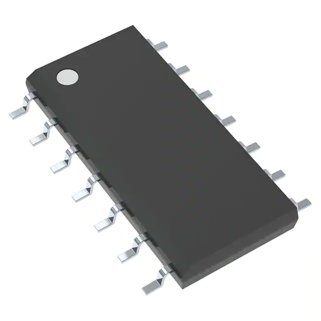
- Part No.:
- NCV4299CD250R2G
- Manufacturer:
- onsemi
- Package:
- 14-SOIC (0.154", 3.90mm Width)
- Datasheet:
-
 NCV4299CD250R2G.pdf
- Description:
- IC REG LINEAR 5V 150MA 14SOIC
- Quantity:
- Payment:

- Shipping:

Inventory:2,500
Please send an inquiry. Send us your inquiry, and we will respond immediately.
Product details
Overview
NCV4299CD250R2G from onsemi is a precision automotive-grade low-dropout linear voltage regulator delivering 150 mA at 5.0 V ±2%, with 0.26 V typical dropout at 100 mA, 80 µA quiescent current in active mode, and <1.0 µA in inhibit-off state. It integrates reset output (RO), sense output (SO), adjustable reset threshold (RADJ), and inhibit (INH) for microprocessor supervision in battery-powered automotive control modules.
For engineers reviewing the NCV4299CD250R2G datasheet, pinout, applications, or equivalent options, this page provides verified technical context, SO-14 pin mapping, AEC-Q100 Grade 1 compliance details, fault protection specs (60 V load dump, −40 V reverse voltage), and real-world design implications for automotive power management.
Technical Context
The NCV4299CD250R2G uses a PNP pass transistor architecture to achieve ultra-low dropout (0.26 V typ. @100 mA) while maintaining ±2% output accuracy across −40 °C to +150 °C. Its internal bandgap reference and saturation-sense circuitry enable stable regulation under wide input transients (VI = 5.5–45 V for 5 V version).
It embeds three independent supervisory functions: (1) RO - open-collector NPN reset output with programmable delay (via external CD capacitor) and operation down to VQ = 1.0 V; (2) SI/SO - early-warning comparator with 1.36 V nominal trip point and 90 mV hysteresis; (3) INH - logic-controlled shutdown reducing Iq to <1.0 µA, available only on SO-14 package variants like NCV4299CD250R2G.
Key Specifications
| Parameter | Value and Actual Design Meaning |
|---|---|
| Output Voltage | 5.0 V ±2% - ensures reliable microprocessor core voltage under temperature and line variation without external trimming. |
| Max Dropout Voltage | 0.50 V @100 mA - enables operation with minimal headroom (e.g., 5.5 V min input), critical for cold-crank automotive conditions. |
| Quiescent Current | 80 µA @100 µA load - extends battery life in always-on vehicle modules (e.g., body control units, telematics). |
| Reset Threshold | 4.67 V typ. (adjustable to 3.5 V via RADJ) - allows precise power-fail detection aligned with MCU brown-out levels. |
| Load Dump Withstand | 60 V peak transient - meets ISO 16750-2 Class C requirements for 12 V automotive systems without external clamping. |
| Operating Temp Range | −40 °C to +150 °C junction - supports under-hood placement per AEC-Q100 Grade 1 qualification. |
| Inhibit Current (Off) | <1.0 µA - enables zero-power sleep states in infotainment or gateway ECUs during vehicle ignition-off. |
Pinout & Package
NCV4299CD250R2G is housed in a Pb-free SOIC-14 (Case 751A, D2 suffix) package with internally fused leads. Thermal resistance is RθJA = 142.7 °C/W (2 oz copper, 150 mm² area), enabling operation up to 150 °C junction temperature without heatsink in moderate-power applications.
| Pin/Terminal | Circuit Role | Design Meaning |
|---|---|---|
| RADJ | Reset Adjust Input | Accepts resistor divider from Q to set custom reset threshold as low as 3.5 V; connect to GND for default 4.67 V. |
| D | Reset Delay Capacitor Node | Sinks 7.1 µA charge current to set power-on-reset delay (e.g., 28 ms with 100 nF); discharges during undervoltage events. |
| GND (Pins 3,4,5,10,11,12) | Ground Reference | Six dedicated ground pins minimize IR drop and improve noise immunity in high-noise automotive environments. |
| INH | Inhibit Control Input | Logic-high enables regulation; logic-low disables output and reduces Iq to <1.0 µA - unique to SO-14 variant. |
| RO | Reset Output (Open Collector) | NPN collector pulled up internally to Q (20 kΩ); asserts low when VQ falls below threshold - directly interfaces MCU reset pin. |
| SO | Sense Output (Open Collector) | NPN collector pulled up internally to Q (20 kΩ); provides early-warning signal before RO assertion - enables graceful MCU shutdown. |
| Q | Regulated Output | 5.0 V ±2% @150 mA; requires ≥22 µF output capacitor with ESR ≤4 Ω for stability across full temp range. |
| I | Input Supply | Battery input (VI = 5.5–45 V); bypass with ceramic capacitor near pin to suppress high-frequency noise. |
| SI | Sense Input | Comparator input referenced to 1.36 V bandgap; used with external resistors to program early-warning trip point for SO. |
Key Features
| Feature | Design Value |
|---|---|
| AEC-Q100 Grade 1 Qualified | Validated for −40 °C to +150 °C operation - certified for engine bay and transmission control unit deployment. |
| Integrated Inhibit Function | Reduces total system standby current to sub-µA levels - essential for meeting OEM "parking mode" current budgets. |
| Programmable Reset Delay & Threshold | Delay set by external capacitor (td ≈ [CD × (1.85 V − 0.1 V)] / 7.1 µA); threshold adjusted via resistor divider on RADJ. |
| Early-Warning Sense Monitor (SI/SO) | Provides >1 µs warning window before reset assertion - allows MCU to save state, flush buffers, and enter safe shutdown. |
| Fault Protection Suite | Includes reverse-battery (−40 V), short-circuit, thermal overload, and 60 V load dump tolerance - eliminates need for discrete protection components. |
Applications
| Body Control Module (BCM) | Advanced Driver Assistance Systems (ADAS) Camera ECU |
|---|---|
Use Scenario: Powering 3.3 V/5.0 V microcontrollers and CAN transceivers in door modules, lighting controllers, and seat memory systems. IC Role / Device Role / Timing Role: Primary 5.0 V LDO with integrated reset and inhibit for MCU supervision and low-power sleep/wake cycles. Use Value: Enables <1.0 µA shutdown current and robust cold-crank operation (VI down to 5.5 V), meeting OEM BCM current consumption targets. |
Use Scenario: Regulating power for image signal processors and SerDes links in rear-view or surround-view camera ECUs. IC Role / Device Role / Timing Role: Stable 5.0 V supply with early-warning SO output to trigger controlled image buffer flush before power loss. Use Value: Prevents corrupted frame capture during battery transients by providing >1 µs advance notice before reset assertion. |
| Telematics Control Unit (TCU) | Electric Power Steering (EPS) Sensor Interface |
Use Scenario: Supplying 5.0 V to cellular modems, GNSS receivers, and secure boot MCUs in connected vehicle gateways. IC Role / Device Role / Timing Role: Fault-tolerant regulator with 60 V load dump immunity and programmable reset timing for OTA update safety. Use Value: Eliminates need for external TVS diodes and reset supervisors - reduces BOM count and PCB area in space-constrained TCUs. |
Use Scenario: Powering Hall-effect or resolver sensor signal conditioners in EPS motor control assemblies exposed to under-hood heat. IC Role / Device Role / Timing Role: High-temp-stable 5.0 V source with thermal shutdown (TSD = 150–200 °C) and reverse-battery protection. Use Value: Ensures uninterrupted sensor data during cranking and load dump events - critical for ASIL-B functional safety compliance. |
Equivalent & Alternatives
The following parts are listed as comparable options for similar automotive LDO regulator applications.
| Alternative Part | Technical Difference | Application Difference | Selection Advice |
|---|---|---|---|
| NCV8664CD2RKG | 3.3 V fixed output, 250 mA, 120 µA Iq, no INH or RADJ - SO-8 package only. | Lacks inhibit and adjustable reset; suited for simpler 3.3 V MCU supplies without advanced supervision. | Select when cost-sensitive 3.3 V regulation is needed and early-warning/sleep control are not required. |
| TLV73350PDQNR | 5.0 V fixed, 300 mA, 60 µA Iq, no automotive qualification, no reset/SO/INH - SOT-23-5 package. | Not AEC-Q100 qualified; lacks fault protection and supervisory features - limited to non-safety-critical cabin electronics. | Choose only for non-automotive or interior-only applications where size and ultra-low Iq outweigh reliability requirements. |
Compared with NCV4299CD250R2G, NCV8664CD2RKG offers higher current but omits inhibit and reset adjust, while TLV73350PDQNR trades automotive robustness for smaller footprint and lower quiescent current - neither matches the integrated supervision and Grade 1 thermal performance of NCV4299CD250R2G.
Availability
NCV4299CD250R2G is available at Aetrix Electronics and suitable for automotive body control, ADAS camera ECUs, telematics gateways, and electric power steering sensor interfaces requiring stable component supply across extended temperature and transient conditions.
Supply support for NCV4299CD250R2G includes scheduled delivery planning, volume procurement assistance, BOM continuity management, traceable sourcing, and lifecycle availability coordination for OEM customers, industrial embedded developers, connected-device designers, and electronics production programs.
Manufacturer
onsemi is a global semiconductor leader focused on energy-efficient innovation, with deep expertise in automotive, industrial, and cloud power solutions.
The NCV4299C product line was designed specifically for AEC-Q100-compliant automotive power management - delivering precision regulation, integrated supervision, and extreme environmental resilience for engine control, chassis, and ADAS systems.
FAQ
What is the maximum input voltage the NCV4299CD250R2G can withstand during load dump events?
The NCV4299CD250R2G is rated for 60 V peak transient voltage per ISO 16750-2 Load Dump Test B, making it suitable for 12 V automotive systems without external clamping. This rating is guaranteed by design and validated per AEC-Q100 stress testing - not production-tested, but fully characterized for Class C compliance.
Does the NCV4299CD250R2G support adjustable reset threshold, and how is it configured?
Yes, the NCV4299CD250R2G supports adjustable reset threshold via the RADJ pin. Applying a resistor divider from Q to RADJ lowers the default 4.67 V threshold down to 3.5 V. The relationship follows VTHRES = VRADJ,TH × (RADJ1 + RADJ2) / RADJ2, where VRADJ,TH = 1.36 V nominal. Connect RADJ to GND for fixed threshold operation.
What is the minimum output capacitance required for stability of the NCV4299CD250R2G?
The NCV4299CD250R2G requires a minimum 22 µF output capacitor with ESR ≤4 Ω for guaranteed stability across −40 °C to +150 °C. Aluminum electrolytic capacitors are recommended; ceramic or film types with near-zero ESR may cause oscillation. Stability boundaries are confirmed in Figure 18 and Figure 33 of the datasheet.
How does the inhibit (INH) function operate on the NCV4299CD250R2G, and what is its current draw in off state?
The INH pin on the NCV4299CD250R2G enables logic-controlled shutdown: a high voltage (>3.5 V) turns regulation on, while a low voltage (<0.8 V) disables the output and reduces total quiescent current to <1.0 µA. This feature is exclusive to SO-14 variants like NCV4299CD250R2G and is critical for meeting automotive parking-mode current limits.
Is the NCV4299CD250R2G still actively manufactured, and what is its lifecycle status?
No - the NCV4299CD250R2G is marked DISCONTINUED in the official onsemi datasheet (Page 18, Note 9) and is not recommended for new designs. However, Aetrix Electronics maintains legacy inventory and supports ongoing production programs with traceable, tested stock and lifecycle coordination for existing automotive platforms.
NCV4299CD250R2G Specifications
- Product attributes
- Attribute value
- Manufacturer:
- onsemi
- Series:
- -
- Package/Case:
- 14-SOIC (0.154", 3.90mm Width)
- Packaging:
- Tape & Reel (TR)
- Product Status:
- Active
- Output Configuration:
- Positive
- Output Type:
- Fixed
- Number of Regulators:
- 1
- Voltage - Input (Max):
- 45V
- Voltage - Output (Min/Fixed):
- 5V
- Voltage - Output (Max):
- -
- Voltage Dropout (Max):
- 0.5V @ 100mA
- Current - Output:
- 150mA
- Current - Quiescent (Iq):
- 90 µA
- Current - Supply (Max):
- 2 mA
- PSRR:
- 66dB (100Hz)
- Control Features:
- Reset
- Protection Features:
- Over Current, Over Temperature
- Operating Temperature:
- -40°C ~ 150°C
- Grade:
- Automotive
- Qualification:
- AEC-Q100
- Mounting Type:
- Surface Mount
- Supplier Device Package:
- 14-SOIC
NCV4299CD250R2G FAQ
1.How can I place an order for NCV4299CD250R2G through Aetrix?
Please submit a Request for Quotation (RFQ) for NCV4299CD250R2G on Aetrix. Our sales agent will provide a competitive quotation and guide you through the order confirmation once you accept the terms.
2.Are the price and stock information for NCV4299CD250R2G reliable?
The price and inventory of NCV4299CD250R2G are updated periodically and may fluctuate due to market conditions. Stock and pricing data are typically refreshed every 24 hours. Quotation validity for NCV4299CD250R2G is usually 5 days.
3.What payment methods are accepted for NCV4299CD250R2G?
We accept Wire Transfer, PayPal, Credit Card, Western Union, MoneyGram, and Escrow for NCV4299CD250R2G transactions.
Note: Certain payment methods may incur a processing fee.
4.How is shipping managed for NCV4299CD250R2G?
NCV4299CD250R2G orders can be shipped via leading logistics carriers, including DHL, UPS, FedEx, TNT, or Registered Mail.
Once your NCV4299CD250R2G order is processed, you will receive an email with the shipment details and tracking number.
Note: Tracking information may take up to 24 hours to appear. Express delivery typically takes 3–5 business days.
5.How can I obtain technical support or documentation for NCV4299CD250R2G?
For technical support, including NCV4299CD250R2G datasheets, pinout diagrams, or application guidance, please contact our engineering support team. They can provide detailed documentation and assistance for your NCV4299CD250R2G requirements.
6.How does Aetrix verify that NCV4299CD250R2G is sourced from the original manufacturer or authorized distributors?
All NCV4299CD250R2G products on Aetrix are procured from qualified distributors and authorized channels. Our dedicated quality assurance team conducts strict verification, including traceability checks and, if necessary, third-party testing. This ensures that NCV4299CD250R2G meets industry standards.
7.What is the process for return or replacement of NCV4299CD250R2G?
All NCV4299CD250R2G units undergo pre-shipment inspection (PSI). If there is an issue with NCV4299CD250R2G, returns or replacements are accepted under the following conditions:
1.Quantity discrepancies, incorrect items, or visible external defects (such as breakage or corrosion), acknowledged by Aetrix.
2.The issue is reported within 90 days of delivery.
3.The NCV4299CD250R2G part is unused and in its original packaging.
Return procedure for NCV4299CD250R2G:
1.Submit a request within 90 days.
2.Obtain a Return Material Authorization (RMA) from Aetrix.
NCV4299CD250R2G Tags

-
MIC5504-1.8YM5-TR
Microchip Technology
-
MIC5504-3.3YM5-TR
Microchip Technology

-
MIC5365-3.0YC5-TR
Microchip Technology
-
MIC5365-1.8YC5-TR
Microchip Technology
-
MIC5365-2.5YC5-TR
Microchip Technology
-
MIC5365-3.3YC5-TR
Microchip Technology

-
MIC5365-3.3YD5-TR
Microchip Technology

-
MIC5317-3.3YM5-TR
Microchip Technology

-
TLV1117LV33DCYR
Texas Instruments

-
MIC5317-3.3YMT-TZ
Microchip Technology

-
MIC5528-3.3YMT-TR
Microchip Technology

-
TLV75801PDRVR
Texas Instruments
Tech Hub

Counterfeit components can hide behind convincing markings and passing basic function tests. This engineering reference covers source traceability, external inspection, X-ray, XRF, electrical testing, …

A practical engineering and sourcing framework covering lifecycle verification, lifetime-buy calculations, replacement qualification, supplier checks and counterfeit-risk controls.

TTL and CMOS logic families differ in thresholds, loading, output drive, power and timing. This engineering guide compares 74HC and 74HCT, calculates noise margins and checks 3.3 V/5 V compatibility.

A practical engineering guide to 3.3V and 5V logic compatibility, input thresholds, resistor dividers, translator ICs, MOSFET level shifting, I2C pull-ups, timing limits and power-sequencing risks.

The 74HC595 uses push-pull logic outputs, while the TPIC6B595 uses 50 V open-drain DMOS sinks for higher-power loads. This guide compares timing, current limits, 3.3 V interfacing, load wiring, thermal…

The 74HC595 converts serial data into eight stable parallel outputs. This guide covers pin functions, shift and storage timing, OE and MR behavior, drive-current limits, cascading, voltage compatibilit…

A technical comparison of level-sensitive latches and edge-triggered flip-flops, covering timing windows, setup and hold limits, master–slave operation, time borrowing, race-through, HDL inference and…

A D latch stores one bit while Enable controls when data can pass. This reference covers gate-level operation, truth tables, transparency, setup and hold timing, LE versus OE, common ICs and practical …

An SR latch stores one bit through cross-coupled feedback. This engineering reference covers NOR and NAND implementations, truth tables, forbidden-state recovery, gated operation, switch debouncing, fa…

Latch circuits retain one bit through feedback. This technical reference covers SR and D latches, truth tables, transparency, timing limits, latch-versus-flip-flop behavior, applications and common log…


