
 My Inquiry
 My Account


onsemi NCV8501PDW80R2G
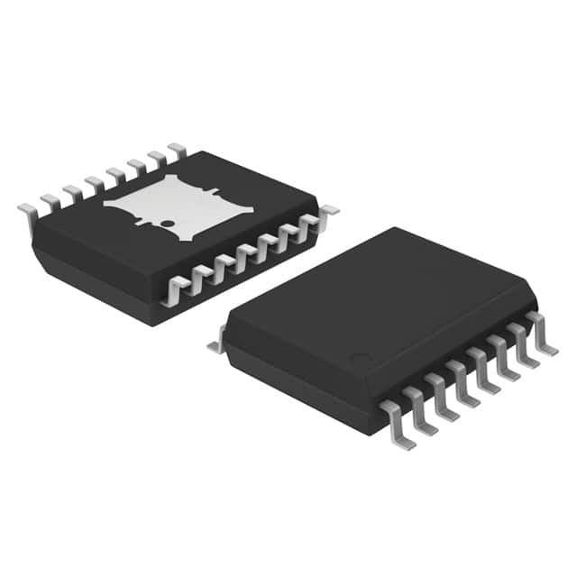
- Part No.:
- NCV8501PDW80R2G
- Manufacturer:
- onsemi
- Package:
- 16-SOIC (0.295", 7.50mm Width) Exposed Pad
- Datasheet:
-
 NCV8501PDW80R2G.pdf
- Description:
- IC REG LINEAR 8V 150MA 16SOIC
- Quantity:
- Payment:

- Shipping:

Inventory:2,492
Please send an inquiry. Send us your inquiry, and we will respond immediately.
Product details
Overview
NCV8501PDW80R2G from onsemi is an automotive-grade 8.0 V fixed-output LDO linear regulator in a SOW-16 exposed pad package, delivering 150 mA output current with ±2.0% accuracy, 0.6 V max dropout at full load, and 90 µA quiescent current under light load - designed for battery-powered microprocessor systems requiring RESET, ENABLE, FLAG monitor, and robust fault protection.
For engineers reviewing the NCV8501PDW80R2G datasheet, pinout, applications, or equivalent options, key selection criteria include its 8.0 V output stability over −40 °C to +150 °C, early-warning FLAG functionality tied to MON input, programmable RESET delay via external capacitor, and automotive-qualified transient tolerance (±15 V reverse, +60 V load dump).
Technical Context
The NCV8501PDW80R2G integrates a precision bandgap reference, error amplifier, and independent low-voltage detection circuitry enabling RESET assertion down to VOUT = 1.0 V. Its FLAG comparator monitors the MON pin with 1.20 V typical threshold and 20–100 mV hysteresis, while ENABLE supports direct battery connection with internal pull-down and 2.55 V typical activation threshold.
RESET timing is controlled by an internal current source (2.5 µA typ) charging an external DELAY capacitor; delay time follows tDELAY = CDELAY × (VDT − VRESET_LOW) / ICHARGE. The device features thermal shutdown at 150 °C, short-circuit current limiting (151–300 mA), and reverse-battery protection up to −15 V.
Key Specifications
| Parameter | Value and Actual Design Meaning |
|---|---|
| Output Voltage | Fixed 8.0 V ±2.0% - ensures stable MCU core/peripheral rail within regulation limits across temperature and load. |
| Max Output Current | 150 mA - sufficient for low-power microcontrollers, CAN transceivers, and sensor interfaces without external pass devices. |
| Dropout Voltage | 600 mV max at 150 mA - enables operation from 8.6 V input in automotive cold-crank conditions (e.g., 8.0 V + 0.6 V). |
| Quiescent Current | 90 µA at 100 µA load - extends battery life in always-on vehicle modules like body control units and telematics. |
| RESET Threshold | 7.05 V (rising), 7.00 V (falling) - provides hysteresis to prevent oscillation during brownout recovery. |
| FLAG Monitor Threshold | 1.20 V on MON pin - allows configurable early warning via resistor divider, giving MCU time to save state before RESET. |
| Operating Temp Range | −40 °C to +150 °C - qualified for under-hood and powertrain applications per AEC-Q100 requirements. |
Pinout & Package
SOW-16 exposed pad (Case 751AG) with thermal pad for enhanced heat dissipation; RJA = 56 °C/W, RJP = 35 °C/W (to pin 16). Pin 16 is GND; exposed pad must be soldered to PCB ground plane for thermal and electrical performance.
| Pin/Terminal | Circuit Role | Design Meaning |
|---|---|---|
| 1, 7 | VIN | Main input supply (−15 V to +45 V); withstands +60 V load dump transients. |
| 2, 8 | MON | Monitor input for FLAG comparator; connect to voltage divider for programmable early-warning threshold. |
| 3, 9 | ENABLE | Active-high enable; internal pull-down; 2.55 V typical threshold; tolerates battery-line connection. |
| 4, 10 | DELAY | Capacitor connection point for RESET delay timing; sourced by 2.5 µA current. |
| 5, 13 | GND | Power ground; all GND pins and exposed pad must be connected to system ground. |
| 6, 16 | RESET | Open-collector active-low reset signal; valid down to VOUT = 1.0 V. |
| 7, 1 | FLAG | Open-collector early-warning output; pulled low when MON voltage drops below threshold. |
| 8, 2 | VOUT | Regulated 8.0 V output; ±2.0% accuracy; requires ≥10 µF output capacitor for stability. |
| 3–6, 11, 12, 14, 15 | NC | No-connect pins; must remain unconnected per datasheet. |
Key Features
| Feature | Design Value |
|---|---|
| Automotive qualification | NCV prefix denotes AEC-Q100 stress-tested, with site/change control and PPAP support. |
| Early-warning FLAG | Provides programmable pre-reset alert via MON pin, allowing MCU to complete critical tasks before shutdown. |
| Programmable RESET delay | External DELAY capacitor sets delay time (e.g., 33 nF → ~24 ms), eliminating need for external timers. |
| Fault protection suite | Integrated reverse-battery (−15 V), short-circuit, thermal shutdown (150 °C), and +60 V load dump tolerance. |
| Pb-free & RoHS compliant | G suffix confirms lead-free packaging meeting JEDEC J-STD-020 reflow profiles and environmental standards. |
Applications
| Body Control Module (BCM) | Instrument Cluster Microcontroller |
|---|---|
Use Scenario: Powering 8-bit/32-bit MCUs and LIN/CAN transceivers in door modules, lighting controllers, and seat position memory circuits. IC Role / Device Role / Timing Role: Primary 8.0 V LDO supplying MCU core logic and peripheral I/O; RESET asserts during battery undervoltage to prevent corrupted EEPROM writes. Use Value: FLAG monitor gives 10–100 ms warning before RESET, enabling safe shutdown of window motor drivers and mirror actuators. | Use Scenario: Regulating power for digital gauges, TFT display controllers, and backlight drivers in automotive dashboards. IC Role / Device Role / Timing Role: Fixed 8.0 V rail generator with ENABLE controlled by ignition switch; DELAY capacitor sets 50 ms reset hold-off after key-on. Use Value: 90 µA quiescent current minimizes parasitic drain during vehicle sleep mode, extending battery life beyond ISO 8820-3 requirements. |
| Telematics Control Unit (TCU) | Advanced Driver Assistance Systems (ADAS) Sensor Hub |
Use Scenario: Supplying GPS/GNSS receivers, cellular modems, and secure boot processors in connected car gateways. IC Role / Device Role / Timing Role: Secondary regulated rail isolated from noisy main 12 V bus; MON pin tied to 5 V auxiliary rail to trigger FLAG if backup power fails. Use Value: ±2.0% output accuracy ensures reliable ADC reference for battery voltage monitoring and diagnostic reporting. | Use Scenario: Powering radar preprocessing SoCs, camera ISPs, and inertial measurement units in front/rear ADAS modules. IC Role / Device Role / Timing Role: High-temp-stable 8.0 V supply with RESET asserted only when VOUT falls below 7.00 V - avoids false resets during engine cranking transients. Use Value: 150 °C junction rating and 56 °C/W RJA allow operation in sealed enclosures near engine bays without heatsinks. |
Equivalent & Alternatives
The following parts are listed as comparable options for similar LDO regulator applications.
| Alternative Part | Technical Difference | Application Difference | Selection Advice |
|---|---|---|---|
| NCV8501D80R2G | SO-8 package (RJA = 165 °C/W), no exposed pad; same electrical specs and pinout mapping for VIN, VOUT, GND, ENABLE, RESET, FLAG, MON, DELAY. | Limited to lower-power applications (<50 mA continuous) due to higher thermal resistance; unsuitable for sustained 150 mA loads in high ambient temps. | Select when board space is constrained and thermal load is light; avoid for under-hood use above 85 °C ambient. |
| TLV70780PDRVR | Single-channel 8.0 V LDO (150 mA), 25 µA IQ, but lacks RESET, FLAG, DELAY, and automotive qualification; RJA = 120 °C/W in 6-pin WSON. | No integrated power-good monitoring or reset sequencing; requires external supervisor IC for safety-critical functions. | Choose for cost-sensitive non-automotive applications where RESET/FLAG are handled elsewhere; not drop-in compatible. |
Compared with NCV8501D80R2G, the NCV8501PDW80R2G delivers 3× better thermal performance for sustained 150 mA loads in hot environments, while TLV70780PDRVR offers lower quiescent current but omits essential automotive safety features and requires additional components for system-level monitoring.
Availability
NCV8501PDW80R2G is available at Aetrix Electronics and suitable for automotive body electronics, instrument clusters, and telematics systems requiring stable component supply, long-term lifecycle support, and AEC-Q100-compliant sourcing.
Supply support for NCV8501PDW80R2G includes scheduled delivery planning, volume procurement assistance, BOM continuity management, traceable sourcing, and lifecycle availability coordination for OEM customers, industrial embedded developers, connected-device designers, and electronics production programs.
Manufacturer
onsemi (formerly ON Semiconductor) is a global semiconductor supplier focused on energy-efficient electronics, with leadership in automotive, industrial, cloud, and IoT markets.
The NCV8501 series was developed specifically for automotive microprocessor power management, integrating RESET, FLAG, ENABLE, and robust fault protection into a single LDO to reduce system component count and improve functional safety compliance.
FAQ
What is the maximum input voltage the NCV8501PDW80R2G can withstand during load dump events?
The NCV8501PDW80R2G is rated for +60 V peak transient voltage during load dump events at VIN, as specified in the Maximum Ratings table. This capability is achieved through internal clamping circuitry and allows direct connection to 12 V automotive battery rails without external TVS diodes in most cases. The device maintains regulation and functional integrity throughout the transient, supporting ASIL-B system designs.
Does the NCV8501PDW80R2G require an external capacitor on the DELAY pin, and how is delay time calculated?
Yes, the NCV8501PDW80R2G requires an external capacitor on the DELAY pin to set RESET assertion delay. Delay time follows tDELAY = CDELAY × (VDT − VRESET_LOW) / ICHARGE, where VDT = 1.8 V (typ), VRESET_LOW ≈ 0 V, and ICHARGE = 2.5 µA (typ). For example, a 33 nF capacitor yields ~24 ms delay. The capacitor must be placed close to the DELAY pin with low-ESR characteristics.
Can the FLAG output of the NCV8501PDW80R2G drive a microcontroller GPIO directly?
Yes, the FLAG output of the NCV8501PDW80R2G is an open-collector NPN transistor capable of sinking ≥1 mA at 0.4 V saturation. It can directly interface with standard 3.3 V or 5 V MCU GPIOs using a pull-up resistor (e.g., 10 kΩ to VCC). The FLAG signal goes low when the MON pin voltage falls below the 1.20 V threshold, providing early warning before RESET activation.
What is the minimum output voltage at which the RESET function remains valid for the NCV8501PDW80R2G?
The RESET function of the NCV8501PDW80R2G remains valid down to VOUT = 1.0 V, as confirmed in the datasheet's "RESET Function" section. This ensures reliable reset signaling even during deep brownout conditions, such as automotive battery sag during cranking. The RESET output is functionally independent of the main regulator loop, guaranteeing deterministic behavior below normal regulation range.
How does the ENABLE pin of the NCV8501PDW80R2G behave when left floating?
When left floating, the ENABLE pin of the NCV8501PDW80R2G is internally pulled down, placing the device in low-IQ sleep mode (≤30 µA). However, the datasheet explicitly recommends against relying on this for normal operation - an external pulldown resistor or active control is required to ensure predictable startup and fail-safe behavior. Floating ENABLE may cause erratic enable/disable cycling in noisy environments.
NCV8501PDW80R2G Specifications
- Product attributes
- Attribute value
- Manufacturer:
- onsemi
- Series:
- -
- Package/Case:
- 16-SOIC (0.295", 7.50mm Width) Exposed Pad
- Packaging:
- Tape & Reel (TR)
- Product Status:
- Obsolete
- Output Configuration:
- Positive
- Output Type:
- Fixed
- Number of Regulators:
- 1
- Voltage - Input (Max):
- 45V
- Voltage - Output (Min/Fixed):
- 8V
- Voltage - Output (Max):
- -
- Voltage Dropout (Max):
- 0.6V @ 150mA
- Current - Output:
- 150mA
- Current - Quiescent (Iq):
- 150 µA
- Current - Supply (Max):
- 19 mA
- PSRR:
- -
- Control Features:
- Enable, Reset
- Protection Features:
- Over Temperature, Reverse Polarity, Short Circuit
- Operating Temperature:
- -40°C ~ 150°C
- Grade:
- Automotive
- Qualification:
- AEC-Q100
- Mounting Type:
- Surface Mount
- Supplier Device Package:
- 16-SOIC
NCV8501PDW80R2G FAQ
1.How can I place an order for NCV8501PDW80R2G through Aetrix?
Please submit a Request for Quotation (RFQ) for NCV8501PDW80R2G on Aetrix. Our sales agent will provide a competitive quotation and guide you through the order confirmation once you accept the terms.
2.Are the price and stock information for NCV8501PDW80R2G reliable?
The price and inventory of NCV8501PDW80R2G are updated periodically and may fluctuate due to market conditions. Stock and pricing data are typically refreshed every 24 hours. Quotation validity for NCV8501PDW80R2G is usually 5 days.
3.What payment methods are accepted for NCV8501PDW80R2G?
We accept Wire Transfer, PayPal, Credit Card, Western Union, MoneyGram, and Escrow for NCV8501PDW80R2G transactions.
Note: Certain payment methods may incur a processing fee.
4.How is shipping managed for NCV8501PDW80R2G?
NCV8501PDW80R2G orders can be shipped via leading logistics carriers, including DHL, UPS, FedEx, TNT, or Registered Mail.
Once your NCV8501PDW80R2G order is processed, you will receive an email with the shipment details and tracking number.
Note: Tracking information may take up to 24 hours to appear. Express delivery typically takes 3–5 business days.
5.How can I obtain technical support or documentation for NCV8501PDW80R2G?
For technical support, including NCV8501PDW80R2G datasheets, pinout diagrams, or application guidance, please contact our engineering support team. They can provide detailed documentation and assistance for your NCV8501PDW80R2G requirements.
6.How does Aetrix verify that NCV8501PDW80R2G is sourced from the original manufacturer or authorized distributors?
All NCV8501PDW80R2G products on Aetrix are procured from qualified distributors and authorized channels. Our dedicated quality assurance team conducts strict verification, including traceability checks and, if necessary, third-party testing. This ensures that NCV8501PDW80R2G meets industry standards.
7.What is the process for return or replacement of NCV8501PDW80R2G?
All NCV8501PDW80R2G units undergo pre-shipment inspection (PSI). If there is an issue with NCV8501PDW80R2G, returns or replacements are accepted under the following conditions:
1.Quantity discrepancies, incorrect items, or visible external defects (such as breakage or corrosion), acknowledged by Aetrix.
2.The issue is reported within 90 days of delivery.
3.The NCV8501PDW80R2G part is unused and in its original packaging.
Return procedure for NCV8501PDW80R2G:
1.Submit a request within 90 days.
2.Obtain a Return Material Authorization (RMA) from Aetrix.
NCV8501PDW80R2G Tags

-
MIC5504-1.8YM5-TR
Microchip Technology
-
MIC5504-3.3YM5-TR
Microchip Technology

-
MIC5365-3.0YC5-TR
Microchip Technology
-
MIC5365-1.8YC5-TR
Microchip Technology
-
MIC5365-2.5YC5-TR
Microchip Technology
-
MIC5365-3.3YC5-TR
Microchip Technology

-
MIC5365-3.3YD5-TR
Microchip Technology

-
MIC5317-3.3YM5-TR
Microchip Technology

-
TLV1117LV33DCYR
Texas Instruments

-
MIC5317-3.3YMT-TZ
Microchip Technology

-
MIC5528-3.3YMT-TR
Microchip Technology

-
TLV75801PDRVR
Texas Instruments
Tech Hub

Counterfeit components can hide behind convincing markings and passing basic function tests. This engineering reference covers source traceability, external inspection, X-ray, XRF, electrical testing, …

A practical engineering and sourcing framework covering lifecycle verification, lifetime-buy calculations, replacement qualification, supplier checks and counterfeit-risk controls.

TTL and CMOS logic families differ in thresholds, loading, output drive, power and timing. This engineering guide compares 74HC and 74HCT, calculates noise margins and checks 3.3 V/5 V compatibility.

A practical engineering guide to 3.3V and 5V logic compatibility, input thresholds, resistor dividers, translator ICs, MOSFET level shifting, I2C pull-ups, timing limits and power-sequencing risks.

The 74HC595 uses push-pull logic outputs, while the TPIC6B595 uses 50 V open-drain DMOS sinks for higher-power loads. This guide compares timing, current limits, 3.3 V interfacing, load wiring, thermal…

The 74HC595 converts serial data into eight stable parallel outputs. This guide covers pin functions, shift and storage timing, OE and MR behavior, drive-current limits, cascading, voltage compatibilit…

A technical comparison of level-sensitive latches and edge-triggered flip-flops, covering timing windows, setup and hold limits, master–slave operation, time borrowing, race-through, HDL inference and…

A D latch stores one bit while Enable controls when data can pass. This reference covers gate-level operation, truth tables, transparency, setup and hold timing, LE versus OE, common ICs and practical …

An SR latch stores one bit through cross-coupled feedback. This engineering reference covers NOR and NAND implementations, truth tables, forbidden-state recovery, gated operation, switch debouncing, fa…

Latch circuits retain one bit through feedback. This technical reference covers SR and D latches, truth tables, transparency, timing limits, latch-versus-flip-flop behavior, applications and common log…


