
 My Inquiry
 My Account


onsemi NCV97311MW50AR2G
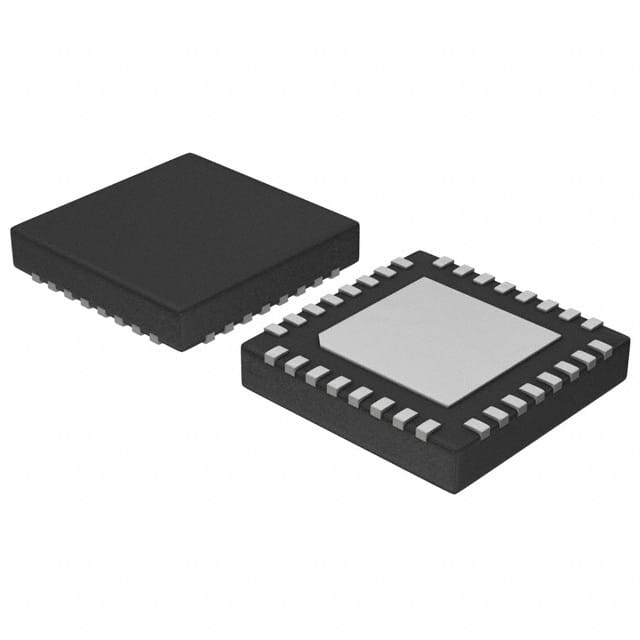
- Part No.:
- NCV97311MW50AR2G
- Manufacturer:
- onsemi
- Category:
- Voltage Regulators - Linear + Switching
- Package:
- 32-VFQFN Exposed Pad
- Datasheet:
-
 NCV97311MW50AR2G.pdf
- Description:
- IC REG QUAD BUCK/LNR SYNC 32QFNW
- Quantity:
- Payment:

- Shipping:

Inventory:1,283
Please send an inquiry. Send us your inquiry, and we will respond immediately.
Product details
Overview
NCV97311MW50AR2G from onsemi is an automotive-grade, battery-connected 3-output power management IC comprising a 3 A, 2 MHz non-synchronous buck regulator (5.0 V fixed output), two 1.5 A, 2 MHz synchronous buck regulators (adjustable 1.2–3.3 V), and a parallel 150 mA low-Iq LDO with 30 µA standby current. It operates from 4.1 V to 34 V input, supports load dump survival up to 45 V, and integrates spread spectrum EMI reduction - deployed in infotainment and body control ECUs.
For engineers reviewing the NCV97311MW50AR2G datasheet, pinout, applications, or equivalent options, key selection considerations include its AEC-Q100 qualification, 5.0 V fixed main rail with minimum-load RMIN support, independent enable/reset per channel, and QFNW32 wettable-flank package for automotive thermal and reliability requirements.
Technical Context
The NCV97311MW50AR2G implements peak-current-mode control with internal slope compensation across all three SMPS channels, using a shared oscillator adjustable from 2.0–2.6 MHz via ROSC. Switcher 1 features foldback to 1 MHz under overvoltage (>18 V) and shutdown at >37 V, while switchers 2/3 remain at nominal frequency during such events.
It integrates dedicated bootstrap supplies (VDRV1/VDRV2), individual FB pins for output adjustability, and three open-drain reset outputs (RSTB1–RSTB3) with programmable delay via external current-setting resistors. The RMIN pin enables minimum-load pull-down specifically for the 5.0 V version, activated above 7.5 V VBAT.
Key Specifications
| Parameter | Value and Actual Design Meaning |
|---|---|
| Output 1 | Fixed 5.0 V @ 3 A; supports battery-connected operation from 4.1–34 V input with UVLO (4.85 V start) and OV shutdown (37 V) |
| Outputs 2 & 3 | Adjustable 1.2–3.3 V @ 1.5 A each; powered from VOUT1; independent EN/RSTB pins enable staggered sequencing |
| Standby Iq | 35 µA typical (VBAT = 13.2 V); achieved by disabling switchers 2/3 and enabling parallel 150 mA LDO with 30 µA quiescent draw |
| Switching Frequency | 2.0 MHz nominal (adjustable 2.0–2.6 MHz via ROSC); spread spectrum enabled via RMOD/RDEPTH resistors (5–50 kHz mod freq, 3–30% depth) |
| Package & Thermal | QFNW32 (5 mm × 5 mm, wettable flanks, exposed pad); RθJA = 25 °C/W; rated for −40 °C to +150 °C junction temperature |
| Protection Features | Cycle-by-cycle current limiting, hiccup-mode OCP, thermal shutdown (150 °C warning, 190 °C shutdown), and error flag (ERRB) combining VIN/VOUT/TEMP faults |
Pinout & Package
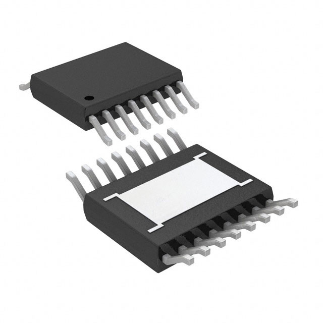
NCV97311MW50AR2G uses a 32-pin QFNW (wettable flanks) package (Case 484AB), with exposed thermal pad electrically connected to GND1 and requiring low-thermal-resistance PCB layout. Pin functions are validated per onsemi datasheet Rev. 6 (May 2025).
| Pin/Terminal | Circuit Role | Design Meaning |
|---|---|---|
| 1, 29 (VBAT, VINL) | Battery input pair | Must be shorted externally; accepts 4.1–45 V; powers switcher 1 and LDO; survives 45 V load dump |
| 2 (EN) | Master enable | TTL-compatible; grounding disables all outputs and reduces Iq to <12 µA (shutdown mode) |
| 3 (STBYB) | Standby mode select | Grounding activates low-Iq LDO mode for VOUT1; disables switchers 2/3; enables 150 mA standby rail |
| 6, 11, 13 (RSTB1–RSTB3) | Open-drain reset outputs | Assert low when respective output falls below 92.5% (RSTB1) or 93.5% (RSTB2/RSTB3) of nominal; delay programmable via pull-up current |
| 26 (RMIN) | Minimum-load pull-down | 5.0 V version only; connects to VOUT1 via resistor to ensure stability under light loads; activated above 7.5 V VBAT |
Key Features
| Feature | Design Value |
|---|---|
| AEC-Q100 Grade 0 qualification | Validated for −40 °C to +150 °C operation; meets automotive reliability, ESD (2 kV HBM), and PPAP requirements |
| Integrated spread spectrum | Reduces peak EMI by sweeping switching frequency up to ±30% around 2 MHz base; configured via RMOD/RDEPTH resistors |
| Independent power sequencing | Three dedicated enable (EN, EN2, EN3) and reset (RSTB1–RSTB3) pins allow precise startup/shutdown timing across domains |
| Robust fault handling | Hiccup-mode OCP, thermal warning (150 °C), full shutdown (190 °C), and ERRB flag combine diagnostics for system-level safety monitoring |
| Wettable-flank QFN package | Enables automated optical inspection (AOI) of solder joints; improves thermal dissipation and mechanical reliability in automotive vibration environments |
Applications
| Infotainment Head Unit Power | Body Control Module (BCM) |
|---|---|
Use Scenario: Powers SoC core, DDR memory, and display interface in 12 V automotive infotainment systems with strict EMI limits. IC Role / Device Role / Timing Role: Primary PMIC delivering 5.0 V main rail to SoC and two adjustable rails (e.g., 1.8 V for DDR, 3.3 V for interface) with spread spectrum to meet CISPR 25 Class 5 radiated emissions. Use Value: Eliminates need for external EMI filters; RMIN ensures stable 5.0 V regulation at light loads during display sleep modes. |
Use Scenario: Supplies microcontroller, CAN transceiver, and sensor interfaces in distributed BCM nodes with variable load profiles. IC Role / Device Role / Timing Role: Provides sequenced 5.0 V MCU core rail and dual 3.3 V/2.5 V peripheral rails; STBYB enables ultra-low-power wake-on-CAN mode. Use Value: 35 µA standby Iq extends battery life during vehicle sleep; independent RSTB outputs enable domain-specific reset coordination. |
| Telematics Control Unit (TCU) | Advanced Driver Assistance Systems (ADAS) Sensor Hub |
Use Scenario: Powers LTE modem, GNSS receiver, and secure element in always-on telematics gateways requiring high reliability. IC Role / Device Role / Timing Role: Delivers fault-tolerant 5.0 V rail with OV/UV protection and ERRB diagnostics; switchers 2/3 supply isolated 1.2 V modem core and 3.3 V RF front-end. Use Value: Survives 45 V load dump events without latch-up; hiccup OCP prevents thermal runaway during antenna mismatch faults. |
Use Scenario: Supplies image signal processor (ISP), radar MMIC bias, and CAN FD interface in compact ADAS sensor fusion hubs. IC Role / Device Role / Timing Role: Generates tightly regulated 5.0 V ISP core, 1.2 V digital logic, and 3.3 V analog bias rails; soft-start (1.4 ms) prevents inrush-induced voltage droop on shared battery. Use Value: Internal slope compensation ensures stable operation across wide input (6–16 V) and load transients; wettable flanks guarantee solder joint integrity under thermal cycling. |
Equivalent & Alternatives
The following parts are listed as comparable options for similar multi-rail automotive PMIC applications.
| Alternative Part | Technical Difference | Application Difference | Selection Advice |
|---|---|---|---|
| NCV97311MW33AR2G | Identical architecture and pinout; fixed 3.3 V main output instead of 5.0 V; RMIN pin is NC (no-connect) | Used where primary SoC requires 3.3 V core rail; not suitable for 5.0 V-dependent peripherals or legacy interfaces | Select only if system architecture mandates 3.3 V main rail; no PCB change required but RMIN must remain floating |
| MPQ4331-AEC1 (Monolithic Power) | Single 3 A buck (no secondary switchers or LDO); AEC-Q100 Grade 1 (−40 °C to +125 °C); no spread spectrum or RSTB outputs | Suitable for simpler single-rail applications; lacks integrated sequencing, diagnostics, or multi-output capability | Use only as partial functional substitute where secondary rails are generated externally; requires additional ICs for full NCV97311MW50AR2G functionality |
Compared with NCV97311MW33AR2G, the NCV97311MW50AR2G provides guaranteed 5.0 V regulation with RMIN support for light-load stability, while MPQ4331-AEC1 offers higher efficiency in single-rail use cases but omits critical automotive features like triple-rail sequencing, ERRB diagnostics, and load-dump survivability.
Availability
NCV97311MW50AR2G is available at Aetrix Electronics and suitable for infotainment head units, body control modules, and telematics control units requiring stable component supply across extended automotive temperature ranges and long production lifecycles.
Supply support for NCV97311MW50AR2G includes scheduled delivery planning, volume procurement assistance, BOM continuity management, traceable sourcing, and lifecycle availability coordination for OEM customers, industrial embedded developers, connected-device designers, and electronics production programs.
Manufacturer
onsemi is a global semiconductor supplier focused on energy-efficient technologies for automotive, industrial, cloud, and IoT applications, with leadership in power management and AEC-Q100 qualified components.
The NCV97311A product line delivers integrated, battery-connected multi-output PMICs optimized for automotive ECU power architectures - emphasizing low-Iq, robust fault protection, and EMI compliance in harsh electrical environments.
FAQ
What is the purpose of the RMIN pin on the NCV97311MW50AR2G?
The RMIN pin is exclusive to the 5.0 V version (NCV97311MW50AR2G) and provides a minimum-load pull-down function to ensure stable regulation under light-load conditions. It activates when VBAT exceeds 7.5 V and must be connected to VOUT1 via an external resistor; this feature is not present in the 3.3 V variant, where RMIN is a no-connect.
Does the NCV97311MW50AR2G support spread spectrum EMI reduction?
Yes, the NCV97311MW50AR2G integrates programmable spread spectrum to reduce peak radiated emissions. Modulation frequency (5–50 kHz) and depth (3–30% of fSW) are set independently via resistors on RMOD and RDEPTH pins, enabling compliance with stringent automotive EMI standards like CISPR 25 without external filtering.
How does the NCV97311MW50AR2G handle overvoltage and load dump conditions?
The NCV97311MW50AR2G shuts down all switching regulators when VBAT exceeds 37 V (OV stop threshold) and survives up to 45 V load dump events. It also implements frequency foldback to 1 MHz between 18–20 V to maintain regulation during overvoltage transients, while the LDO and internal circuitry remain protected per AEC-Q100 stress requirements.
Can the NCV97311MW50AR2G operate in ultra-low-power standby mode?
Yes, the NCV97311MW50AR2G achieves 35 µA typical quiescent current in standby mode by grounding STBYB to disable switchers 2 and 3 and activate the parallel 150 mA LDO. This mode maintains a regulated 5.0 V rail for critical wake-up circuitry while minimizing battery drain during vehicle sleep cycles.
Is the NCV97311MW50AR2G pin-compatible with other variants in the NCV97311A family?
Yes, all NCV97311A variants-including NCV97311MW50AR2G and NCV97311MW33AR2G-share identical QFNW32 pinout, package, and footprint. The only functional difference is the fixed output voltage (5.0 V vs. 3.3 V) and RMIN pin usage; no PCB redesign is needed when migrating between these versions.
NCV97311MW50AR2G Specifications
- Product attributes
- Attribute value
- Manufacturer:
- onsemi
- Series:
- -
- Package/Case:
- 32-VFQFN Exposed Pad
- Packaging:
- Tape & Reel (TR)
- Product Status:
- Active
- Topology:
- Step-Down (Buck) Synchronous (2), Linear (LDO) (2)
- Number of Outputs:
- 4
- Frequency - Switching:
- 2MHz ~ 2.6MHz
- Voltage/Current - Output 1:
- 5V, 3A
- Voltage/Current - Output 2:
- 1.2V ~ 3.3V, 1.5A
- Voltage/Current - Output 3:
- 1.2V ~ 3.3V, 1.5A
- w/LED Driver:
- No
- w/Supervisor:
- No
- w/Sequencer:
- No
- Voltage - Supply:
- 4.1V ~ 18V
- Operating Temperature:
- -40°C ~ 125°C (TA)
- Grade:
- Automotive
- Qualification:
- AEC-Q100
- Mounting Type:
- Surface Mount, Wettable Flank
- Supplier Device Package:
- 32-QFNW (5x5)
NCV97311MW50AR2G FAQ
1.How can I place an order for NCV97311MW50AR2G through Aetrix?
Please submit a Request for Quotation (RFQ) for NCV97311MW50AR2G on Aetrix. Our sales agent will provide a competitive quotation and guide you through the order confirmation once you accept the terms.
2.Are the price and stock information for NCV97311MW50AR2G reliable?
The price and inventory of NCV97311MW50AR2G are updated periodically and may fluctuate due to market conditions. Stock and pricing data are typically refreshed every 24 hours. Quotation validity for NCV97311MW50AR2G is usually 5 days.
3.What payment methods are accepted for NCV97311MW50AR2G?
We accept Wire Transfer, PayPal, Credit Card, Western Union, MoneyGram, and Escrow for NCV97311MW50AR2G transactions.
Note: Certain payment methods may incur a processing fee.
4.How is shipping managed for NCV97311MW50AR2G?
NCV97311MW50AR2G orders can be shipped via leading logistics carriers, including DHL, UPS, FedEx, TNT, or Registered Mail.
Once your NCV97311MW50AR2G order is processed, you will receive an email with the shipment details and tracking number.
Note: Tracking information may take up to 24 hours to appear. Express delivery typically takes 3–5 business days.
5.How can I obtain technical support or documentation for NCV97311MW50AR2G?
For technical support, including NCV97311MW50AR2G datasheets, pinout diagrams, or application guidance, please contact our engineering support team. They can provide detailed documentation and assistance for your NCV97311MW50AR2G requirements.
6.How does Aetrix verify that NCV97311MW50AR2G is sourced from the original manufacturer or authorized distributors?
All NCV97311MW50AR2G products on Aetrix are procured from qualified distributors and authorized channels. Our dedicated quality assurance team conducts strict verification, including traceability checks and, if necessary, third-party testing. This ensures that NCV97311MW50AR2G meets industry standards.
7.What is the process for return or replacement of NCV97311MW50AR2G?
All NCV97311MW50AR2G units undergo pre-shipment inspection (PSI). If there is an issue with NCV97311MW50AR2G, returns or replacements are accepted under the following conditions:
1.Quantity discrepancies, incorrect items, or visible external defects (such as breakage or corrosion), acknowledged by Aetrix.
2.The issue is reported within 90 days of delivery.
3.The NCV97311MW50AR2G part is unused and in its original packaging.
Return procedure for NCV97311MW50AR2G:
1.Submit a request within 90 days.
2.Obtain a Return Material Authorization (RMA) from Aetrix.
NCV97311MW50AR2G Tags

-
TPS6521905RHBR
Texas Instruments
-
MIC3385YHL-TR
Microchip Technology
-
A4402ELPTR-T
Allegro MicroSystems

-
LM26480SQ-AA/NOPB
Texas Instruments
-
A4402KLPTR-T
Allegro MicroSystems
-
BD71847AMWV-E2
ROHM Semiconductor
-
ADP5040ACPZ-1-R7
Analog Devices Inc.
-
LT3048IDC#TRPBF
Analog Devices Inc.
-
ADP5037ACPZ-R7
Analog Devices Inc.

-
XRP7714ILB-F
MaxLinear, Inc.
-
LTC3260EDE#TRPBF
Analog Devices Inc.
-
LTC3260EMSE#PBF
Analog Devices Inc.
Tech Hub

Counterfeit components can hide behind convincing markings and passing basic function tests. This engineering reference covers source traceability, external inspection, X-ray, XRF, electrical testing, …

A practical engineering and sourcing framework covering lifecycle verification, lifetime-buy calculations, replacement qualification, supplier checks and counterfeit-risk controls.

TTL and CMOS logic families differ in thresholds, loading, output drive, power and timing. This engineering guide compares 74HC and 74HCT, calculates noise margins and checks 3.3 V/5 V compatibility.

A practical engineering guide to 3.3V and 5V logic compatibility, input thresholds, resistor dividers, translator ICs, MOSFET level shifting, I2C pull-ups, timing limits and power-sequencing risks.

The 74HC595 uses push-pull logic outputs, while the TPIC6B595 uses 50 V open-drain DMOS sinks for higher-power loads. This guide compares timing, current limits, 3.3 V interfacing, load wiring, thermal…

The 74HC595 converts serial data into eight stable parallel outputs. This guide covers pin functions, shift and storage timing, OE and MR behavior, drive-current limits, cascading, voltage compatibilit…

A technical comparison of level-sensitive latches and edge-triggered flip-flops, covering timing windows, setup and hold limits, master–slave operation, time borrowing, race-through, HDL inference and…

A D latch stores one bit while Enable controls when data can pass. This reference covers gate-level operation, truth tables, transparency, setup and hold timing, LE versus OE, common ICs and practical …

An SR latch stores one bit through cross-coupled feedback. This engineering reference covers NOR and NAND implementations, truth tables, forbidden-state recovery, gated operation, switch debouncing, fa…

Latch circuits retain one bit through feedback. This technical reference covers SR and D latches, truth tables, transparency, timing limits, latch-versus-flip-flop behavior, applications and common log…


