
 My Inquiry
 My Account


NXP Semiconductors NCX8193GUX
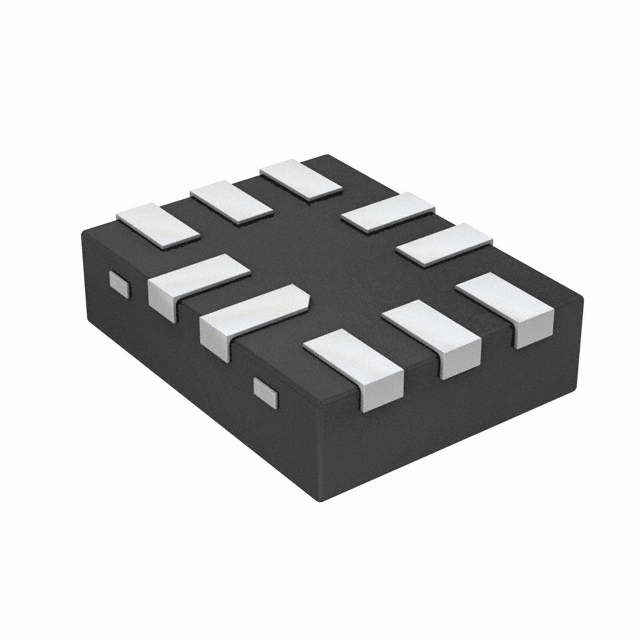
- Part No.:
- NCX8193GUX
- Manufacturer:
- NXP Semiconductors
- Category:
- Audio Special Purpose
- Package:
- 10-XFQFN
- Datasheet:
-
 NCX8193GUX.pdf
- Description:
- IC DETECTION MONITOR 10XQFN
- Quantity:
- Payment:

- Shipping:

Inventory:1,841
Please send an inquiry. Send us your inquiry, and we will respond immediately.
Product details
Overview
NCX8193GUX from NXP Semiconductors is an audio jack accessory detector and controller IC designed for reliable 3-pole and 4-pole plug insertion detection using fault-detection logic. It integrates a microphone bias path switch (RON = 0.9 Ω typ. at 2.8 V), Send/End button detection (780 mV trigger), and low-THD (0.01%) analog pass-through for headset applications in smartphones and portable media devices.
For engineers reviewing the NCX8193GUX datasheet, NCX8193GUX pinout, NCX8193GUX application, or NCX8193GUX equivalent, key selection considerations include its false-detection prevention architecture, J_DET voltage thresholding (400 mV detect / 300 mV confirmation), EN-controlled microphone path switching, and XQFN10 package compatibility with space-constrained mobile PCB layouts.
Technical Context
The NCX8193GUX implements a two-stage plug detection algorithm: J_DET is first pulled up via a 1.2 MΩ resistor; when voltage drops below 400 mV, the pull-up is disabled and a variable current source engages. Sustained J_DET < 300 mV triggers DET = LOW. Button press detection on J_MIC operates independently with a fixed 780 mV reference and supports forward/reverse/call-end event encoding.
Its dual-supply architecture separates core logic (VCC, 2.4–5.25 V) from I/O interface (VCC(IO), 1.6–VCC), enabling codec-side bias control and minimizing interference between detection logic and analog audio paths. The device maintains < 25 µA active-mode supply current and achieves −100 dB OFF-state isolation and −110 dB PSRR for clean microphone signal routing.
Key Specifications
| Parameter | Value and Actual Design Meaning |
|---|---|
| VCC Range | 2.4 V to 5.25 V - supports direct connection to main system battery or LDO output without level-shifting |
| VCC(IO) Range | 1.6 V to VCC - enables independent bias voltage scaling for codec compatibility and noise reduction |
| Plug Detect Threshold | 400 mV (VT−) and 300 mV (Vref) - dual-voltage validation prevents false triggers from moisture or contact bounce |
| Button Detect Threshold | 780 mV ±62 mV - precise level sensing for reliable Send/End and media control button decoding |
| Microphone Switch RON | 0.9 Ω typical at 2.8 V - ultra-low ON resistance minimizes signal attenuation and DC drop in bias path |
| THD | 0.01% at 20 Hz–20 kHz - preserves microphone fidelity across full audio bandwidth with negligible harmonic distortion |
| ESD Protection | HBM Class 3B > 8 kV - robust handling of human-body discharge during assembly and end-user plugging cycles |
Pinout & Package
XQFN10 (SOT1160-2) package: plastic extremely thin quad flat no-lead, 1.8 mm × 1.4 mm × 0.5 mm body, 10-terminal layout optimized for high-density mobile PCBs.
| Pin/Terminal | Circuit Role | Design Meaning |
|---|---|---|
| VCC(IO) | Power | Digital I/O and headphone bias supply - powers DET/S/E outputs and MIC/J_MIC switch logic |
| DET | Output | Active-Low plug-insertion flag - asserts LOW after validated detection sequence completes |
| EN | Input | Microphone bias path enable - HIGH closes MIC-to-J_MIC switch; LOW isolates paths |
| n.c. | No Connect | Not internally bonded - recommended to tie to GND for mechanical stability and EMI control |
| VCC | Power | Core logic supply - powers internal state machine, current sources, and digital control circuitry |
| S/E | Output | Active-High button-press indicator - pulses HIGH upon valid J_MIC voltage transition above 780 mV |
| MIC | I/O | Codec-side microphone interface - receives bias and passes button events to processor |
| J_MIC | I/O | Headset-side microphone interface - connects to headset mic element and button matrix |
| GND | Ground | Common reference for all analog/digital domains - requires low-impedance plane connection |
| J_DET | I/O | Jack detection bias node - senses plug insertion via voltage divider; controlled by internal pull-up/current source |
Key Features
| Feature | Design Value |
|---|---|
| Fail-safe detection logic | Two-stage voltage validation (400 mV → 300 mV) eliminates false triggers from sweat, debris, or partial insertion |
| Click-free switching | Controlled EN timing (15 µs enable/disable) and low-THD path prevent audible pop/click during mic path activation |
| Low-power standby | 0.1 µA ICC(tot) in Sleep mode - extends battery life in always-on detection applications |
| Integrated button decode | Hardware-level 780 mV thresholding and S/E output offload processor interrupt handling for media controls |
| High-reliability bias switch | 0.9 Ω RON with ±0.6 Ω flatness ensures consistent microphone sensitivity across 0.8–1.2 V bias range |
Applications
| Smartphone Headset Interface | Tablet Audio Accessory Hub |
|---|---|
Use Scenario: Detecting TRRS headset insertion and decoding inline remote button presses in Android/iOS-based handsets. IC Role / Device Role / Timing Role: NCX8193GUX acts as the primary jack presence and button-event transducer, interfacing directly with baseband/application processor GPIOs and audio codec MIC inputs. Use Value: Eliminates need for external RC debounce networks and discrete MOSFET switches while maintaining < 40 ms unplug response time and moisture immunity. | Use Scenario: Supporting multi-brand aftermarket headphones with varying impedance and button configurations in portable tablets. IC Role / Device Role / Timing Role: NCX8193GUX serves as universal accessory identification engine, managing J_DET voltage thresholds and J_MIC bias levels per connected headset type. Use Value: Enables broad compatibility with third-party headsets without firmware reconfiguration, leveraging hardware-based 780 mV button detection and 1.2 MΩ adaptive pull-up. |
| Wearable Media Player Dock | USB-C Audio Adapter Module |
Use Scenario: Detecting and configuring wired headset connections in compact wearable players with integrated DAC/AMP. IC Role / Device Role / Timing Role: NCX8193GUX provides plug-in status and mic path control to the wearable's audio subsystem, synchronizing with power management states. Use Value: Reduces BOM count by integrating detection, bias switching, and button decode into single 1.8 × 1.4 mm XQFN10 footprint. | Use Scenario: Adding analog headset support to USB-C dongles that convert digital audio to 3.5 mm TRRS output. IC Role / Device Role / Timing Role: NCX8193GUX bridges USB-C controller GPIOs to legacy headset jack, handling plug detection and mic bias under USB PD power negotiation constraints. Use Value: Maintains low standby current (< 1 µA) during USB suspend while enabling instant wake-on-plug via DET assertion. |
Equivalent & Alternatives
The following parts are listed as comparable options for similar audio jack detection and configuration applications.
| Alternative Part | Technical Difference | Application Difference | Selection Advice |
|---|---|---|---|
| MAX14525ETA+ | Single-supply operation (1.6–3.6 V); lacks dedicated S/E output; uses I²C interface for button reporting | Requires host processor I²C polling instead of GPIO-driven edge interrupts | Prefer when system already uses I²C for accessory management and board space allows TDFN-8 package |
| TPS65987D | USB-C port controller with integrated audio jack detection; higher integration but larger QFN-60 package and complex firmware dependency | Designed for USB-C DRP systems only; not suitable for standalone jack detection | Choose only if USB-C alternate mode and PD control are required alongside jack detection |
Compared with MAX14525ETA+ and TPS65987D, the NCX8193GUX delivers dedicated, GPIO-native plug/button detection in the smallest footprint (1.8 × 1.4 mm), with no firmware overhead and guaranteed moisture-resistant operation - making it optimal for cost-sensitive, space-constrained mobile audio interfaces.
Availability
NCX8193GUX is available at Aetrix Electronics and suitable for smartphone headset interfaces, tablet accessory hubs, wearable media players, and USB-C audio adapters requiring stable component supply and long-term production continuity.
Supply support for NCX8193GUX includes scheduled delivery planning, volume procurement assistance, BOM continuity management, traceable sourcing, and lifecycle availability coordination for OEM customers, industrial embedded developers, connected-device designers, and electronics production programs.
Manufacturer
NXP Semiconductors is a global semiconductor company headquartered in Eindhoven, Netherlands, specializing in secure connectivity solutions for automotive, industrial, and mobile applications.
The NCX8193GUX belongs to NXP's audio interface and accessory detection product line, engineered specifically to replace discrete detection circuits in portable consumer electronics with high-reliability, low-power, and small-footprint integrated solutions.
FAQ
What is the primary function of the NCX8193GUX in a mobile device design?
The NCX8193GUX serves as a dedicated audio jack accessory detector and controller, performing plug insertion detection for 3-pole and 4-pole connectors, managing microphone bias path switching via the EN pin, and detecting Send/End button presses on TRRS headsets. Its core value lies in replacing multiple discrete components with a single IC that ensures robust false-detection prevention and low-THD analog signal integrity - all within the NCX8193GUX's XQFN10 package.
How does the NCX8193GUX prevent false detection due to moisture or partial insertion?
The NCX8193GUX employs a two-stage voltage validation process on the J_DET pin: initial detection occurs at 400 mV, but DET only asserts LOW after sustained voltage remains below 300 mV. This hysteresis-based method rejects transient dips caused by moisture bridging or intermittent contact. The NCX8193GUX also features a programmable 40 ms unplug delay and adaptive current-source ramping to further suppress false triggers - confirmed in its functional description and Table 8 threshold specifications.
What are the supply voltage requirements for the NCX8193GUX, and why are there two separate supplies?
The NCX8193GUX requires two independent supplies: VCC (2.4–5.25 V) for core logic and detection circuitry, and VCC(IO) (1.6 V to VCC) for I/O interface and microphone bias control. This separation isolates noise-sensitive analog paths from digital switching noise, enables flexible codec-side bias voltage scaling, and allows the NCX8193GUX to operate correctly even when VCC(IO) is lower than VCC - a critical feature for mixed-voltage mobile SoC interfaces.
Can the NCX8193GUX support both 3-pole and 4-pole headset configurations, and how is this achieved?
Yes, the NCX8193GUX natively supports both 3-pole (TRS) and 4-pole (TRRS) headset configurations through its J_DET and J_MIC pins, which sense jack topology via resistance and voltage divider behavior. Its detection algorithm adapts to different pole counts by monitoring J_DET voltage transitions and validating against defined thresholds (400 mV/300 mV). The NCX8193GUX datasheet explicitly states this capability in Section 1 and confirms compatibility with "a broad variety of after-market headphones" - including both configurations.
What is the significance of the 780 mV reference voltage in the NCX8193GUX's button detection circuit?
The 780 mV reference voltage is the precise threshold used by the NCX8193GUX to detect button presses on the J_MIC line. When a headset button closes a resistive path, J_MIC voltage rises above this level, causing the S/E output to assert HIGH. The specification guarantees ±62 mV tolerance (718–842 mV) across temperature, ensuring reliable detection across diverse button designs and battery voltages. This hardware-level threshold eliminates software debounce and makes the NCX8193GUX's button response deterministic and low-latency.
NCX8193GUX Specifications
- Product attributes
- Attribute value
- Manufacturer:
- NXP Semiconductors
- Series:
- -
- Package/Case:
- 10-XFQFN
- Packaging:
- Tape & Reel (TR)
- Product Status:
- Obsolete
- Function:
- Detection Monitor
- Applications:
- Communication Systems
- Number of Channels:
- 1
- Interface:
- Analog
- Voltage - Supply:
- 2.4V ~ 5.25V
- Operating Temperature:
- -40°C ~ 85°C (TA)
- Specifications:
- -
- Mounting Type:
- Surface Mount
- Grade:
- -
NCX8193GUX FAQ
1.How can I place an order for NCX8193GUX through Aetrix?
Please submit a Request for Quotation (RFQ) for NCX8193GUX on Aetrix. Our sales agent will provide a competitive quotation and guide you through the order confirmation once you accept the terms.
2.Are the price and stock information for NCX8193GUX reliable?
The price and inventory of NCX8193GUX are updated periodically and may fluctuate due to market conditions. Stock and pricing data are typically refreshed every 24 hours. Quotation validity for NCX8193GUX is usually 5 days.
3.What payment methods are accepted for NCX8193GUX?
We accept Wire Transfer, PayPal, Credit Card, Western Union, MoneyGram, and Escrow for NCX8193GUX transactions.
Note: Certain payment methods may incur a processing fee.
4.How is shipping managed for NCX8193GUX?
NCX8193GUX orders can be shipped via leading logistics carriers, including DHL, UPS, FedEx, TNT, or Registered Mail.
Once your NCX8193GUX order is processed, you will receive an email with the shipment details and tracking number.
Note: Tracking information may take up to 24 hours to appear. Express delivery typically takes 3–5 business days.
5.How can I obtain technical support or documentation for NCX8193GUX?
For technical support, including NCX8193GUX datasheets, pinout diagrams, or application guidance, please contact our engineering support team. They can provide detailed documentation and assistance for your NCX8193GUX requirements.
6.How does Aetrix verify that NCX8193GUX is sourced from the original manufacturer or authorized distributors?
All NCX8193GUX products on Aetrix are procured from qualified distributors and authorized channels. Our dedicated quality assurance team conducts strict verification, including traceability checks and, if necessary, third-party testing. This ensures that NCX8193GUX meets industry standards.
7.What is the process for return or replacement of NCX8193GUX?
All NCX8193GUX units undergo pre-shipment inspection (PSI). If there is an issue with NCX8193GUX, returns or replacements are accepted under the following conditions:
1.Quantity discrepancies, incorrect items, or visible external defects (such as breakage or corrosion), acknowledged by Aetrix.
2.The issue is reported within 90 days of delivery.
3.The NCX8193GUX part is unused and in its original packaging.
Return procedure for NCX8193GUX:
1.Submit a request within 90 days.
2.Obtain a Return Material Authorization (RMA) from Aetrix.
NCX8193GUX Tags

-
SA571DR2G
onsemi
-
ADAU7002ACBZ-R7
Analog Devices Inc.

-
DRV135UA/2K5
Texas Instruments

-
DRV134UA/1K
Texas Instruments

-
DRV134PA
Texas Instruments
-
DRV134UA
Texas Instruments
-
DRV135UA
Texas Instruments
-
SA572DR2G
onsemi
-
PGA2311U/1K
Texas Instruments
-
SI8244BB-D-IS1R
Skyworks Solutions Inc.

-
CS8416K-CZZR
Cirrus Logic Inc.
-
SRC4392IPFBR
Texas Instruments
Tech Hub

A practical engineering guide to 3.3V and 5V logic compatibility, input thresholds, resistor dividers, translator ICs, MOSFET level shifting, I2C pull-ups, timing limits and power-sequencing risks.

The 74HC595 uses push-pull logic outputs, while the TPIC6B595 uses 50 V open-drain DMOS sinks for higher-power loads. This guide compares timing, current limits, 3.3 V interfacing, load wiring, thermal…

The 74HC595 converts serial data into eight stable parallel outputs. This guide covers pin functions, shift and storage timing, OE and MR behavior, drive-current limits, cascading, voltage compatibilit…

A technical comparison of level-sensitive latches and edge-triggered flip-flops, covering timing windows, setup and hold limits, master–slave operation, time borrowing, race-through, HDL inference and…

A D latch stores one bit while Enable controls when data can pass. This reference covers gate-level operation, truth tables, transparency, setup and hold timing, LE versus OE, common ICs and practical …

An SR latch stores one bit through cross-coupled feedback. This engineering reference covers NOR and NAND implementations, truth tables, forbidden-state recovery, gated operation, switch debouncing, fa…

Latch circuits retain one bit through feedback. This technical reference covers SR and D latches, truth tables, transparency, timing limits, latch-versus-flip-flop behavior, applications and common log…

An engineering guide to LED driver operation, constant-current and constant-voltage outputs, linear and switching topologies, dimming, IC selection, calculations, replacement compatibility, and fault c…

Operational amplifier guide covering op amp basics, feedback, ideal vs real op amps, common configurations, buffer circuits, offset, bias current, gain-bandwidth, slew rate, rail-to-rail limits and sel…

Jumper cables guide covering safe connection order, red and black clamp placement, final ground connection, cable gauge, length, clamp quality, copper vs CCA cables, jump starter comparison and battery…


