
 My Inquiry
 My Account


onsemi NL17SG08AMUTCG
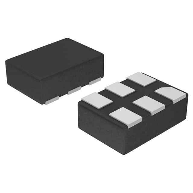
- Part No.:
- NL17SG08AMUTCG
- Manufacturer:
- onsemi
- Category:
- Gates and Inverters
- Package:
- 6-UFDFN
- Datasheet:
-
 NL17SG08AMUTCG.pdf
- Description:
- IC GATE AND 1CH 2-INP 6UDFN
- Quantity:
- Payment:

- Shipping:

Inventory:3,391
Please send an inquiry. Send us your inquiry, and we will respond immediately.
Product details
Overview
NL17SG08AMUTCG from onsemi is a single 2-input CMOS AND gate optimized for ultra-low-voltage operation (0.9 V to 3.6 V VCC), delivering 2.5 ns typical propagation delay at 3.0 V with 15 pF load, over-voltage tolerant I/O up to 3.6 V, IOFF partial power-down protection, and AEC-Q101 qualification for automotive use in compact UDFN6 (1.0 mm × 1.0 mm) package.
For engineers reviewing the NL17SG08AMUTCG datasheet, pinout, applications, or equivalent options, this page provides verified functional identity, validated UDFN6 pin mapping, confirmed 0.9–3.6 V supply range, real-world timing performance at multiple VCC/CL conditions, and direct alternative options with documented technical differences.
Technical Context
The NL17SG08AMUTCG implements a standard positive-logic 2-input AND function with Schmitt-trigger–free inputs and push-pull CMOS output stage. Its input structure supports over-voltage tolerance independent of VCC, enabling safe interfacing with higher-voltage logic domains up to 3.6 V even when VCC = 0.9 V.
IOFF circuitry actively disables input/output paths during power-down (VCC = 0 V), limiting leakage to ≤10 µA while maintaining signal integrity across unpowered sections of mixed-supply systems - critical for battery-backed subsystems and hot-swap interfaces.
Key Specifications
| Parameter | Value and Actual Design Meaning |
|---|---|
| VCC Range | 0.9 V to 3.6 V - enables direct integration into sub-1.0 V logic rails and compatibility with 1.2 V, 1.8 V, 2.5 V, and 3.3 V domains without level shifters. |
| tPLH/tPHL (Typ) | 2.5 ns at VCC = 3.0 V, CL = 15 pF - ensures minimal combinatorial delay in high-speed control path timing budgets. |
| Input Voltage Tolerance | −0.5 V to +4.3 V - allows safe connection to 3.3 V or 3.6 V signals even when VCC is as low as 0.9 V, eliminating external clamping diodes. |
| IOFF Leakage | ≤10.0 µA at VIN/VOUT = 0–3.6 V, VCC = 0 V - prevents back-powering and signal corruption in partial-power-down states. |
| Operating Temperature | −55 °C to +125 °C - supports under-hood automotive, industrial motor control, and extended-range IoT edge nodes. |
| ESD Rating | 2000 V HBM - meets robustness requirements for manual handling and board-level assembly without special ESD controls. |
| Package | UDFN6 (1.0 mm × 1.0 mm, 0.35 mm pitch) - delivers smallest footprint among NL17SG08 variants for space-constrained PCB layouts. |
Pinout & Package
UDFN6 package (Case 517BX), 1.0 mm × 1.0 mm, 0.35 mm pitch, bottom-exposed thermal pad, RoHS-compliant, Pb-free.
| Pin/Terminal | Circuit Role | Design Meaning |
|---|---|---|
| 1 | B (Input) | Second logic input; accepts voltages up to 3.6 V regardless of VCC; internally clamped and over-voltage tolerant. |
| 2 | A (Input) | First logic input; identical electrical behavior to Pin 1; dual-input AND function requires both A and B high for Y assertion. |
| 3 | GND | Ground reference for all internal circuitry and output stage; must be connected to system ground plane for stable operation. |
| 4 | NC | No internal connection; electrically isolated; must remain unconnected per datasheet to avoid parasitic coupling or latch-up risk. |
| 5 | Y (Output) | CMOS push-pull output; drives high/low with ±8 mA capability at 3.0–3.6 V; compatible with standard TTL/CMOS loads. |
| 6 | VCC | Positive supply rail; powers internal logic and output stage; supports dynamic voltage scaling from 0.9 V to 3.6 V. |
Key Features
| Feature | Design Value |
|---|---|
| Ultra-low-voltage operation | Functional down to 0.9 V VCC - enables direct interface with energy-harvesting PMUs and sub-1 V microcontrollers. |
| Over-voltage tolerant I/O | Inputs and outputs withstand −0.5 V to +4.3 V - eliminates need for external voltage translators when bridging 1.8 V logic to 3.3 V peripherals. |
| IOFF partial power-down | Leakage ≤10 µA with VCC = 0 V - preserves isolation between powered/unpowered domains in modular systems and battery-backed memory retention circuits. |
| AEC-Q101 qualified | Validated for automotive applications including engine control modules, body electronics, and ADAS sensor interfaces. |
| Miniature UDFN6 footprint | 1.0 mm × 1.0 mm area - reduces PCB real estate by >50% vs. SC-88A and >65% vs. SOT-953, critical for wearable and portable designs. |
Applications
| Automotive Body Control Module | Industrial Sensor Interface Logic |
|---|---|
|
Use Scenario: Combining door lock status and ignition key presence signals before enabling window lift motor drive enable. IC Role / Device Role / Timing Role: Dual-input AND gate performing safety-critical interlock logic with guaranteed sub-5 ns response at 3.3 V supply. Use Value: Eliminates discrete resistor-diode logic, reduces BOM count, and ensures deterministic timing under temperature extremes (−40 °C to +125 °C). |
Use Scenario: Enabling analog-to-digital converter sampling only when both sensor readiness flag and system clock enable are asserted. IC Role / Device Role / Timing Role: Synchronous gating element synchronizing data acquisition windows with system-level control signals. Use Value: Provides clean, glitch-free enable pulses with <2.5 ns propagation delay variation across 0.9–3.6 V supply range, improving ADC effective resolution. |
| Low-Power Wearable Power Sequencing | IoT Edge Node Wake-Up Logic |
|
Use Scenario: AND-ing motion-detection interrupt and BLE radio ready signal to trigger MCU wake-up from deep sleep. IC Role / Device Role / Timing Role: Ultra-low-voltage combinational logic block operating at 0.9 V to minimize quiescent current (<10 µA ICC). Use Value: Enables full-system wake-up within 3 ns of event detection while consuming <0.5 µW static power - extending coin-cell battery life by >30%. |
Use Scenario: Gating environmental sensor readout to prevent transmission until both humidity and temperature thresholds are exceeded. IC Role / Device Role / Timing Role: Threshold coordination logic using two independent sensor outputs as inputs to generate composite alert signal. Use Value: Reduces false alerts by requiring concurrent sensor conditions, with over-voltage tolerant inputs allowing direct connection to 3.3 V sensor outputs even when MCU runs at 1.8 V. |
Equivalent & Alternatives
The following parts are listed as comparable options for similar 2-input AND gate applications.
| Alternative Part | Technical Difference | Application Difference | Selection Advice |
|---|---|---|---|
| SN74LVC1G08DBVR | Wider VCC range (1.65–5.5 V); no IOFF; 3.5 ns tPLH at 3.3 V/15 pF; SOT-23-5 package (2.9 mm × 1.6 mm). | Not qualified for automotive; lacks partial power-down protection; larger footprint limits high-density layouts. | Select when interfacing with 5 V legacy peripherals or when IOFF is unnecessary and cost is primary driver. |
| 74LVC1G08GW,125 | VCC = 1.65–5.5 V; no over-voltage tolerance beyond VCC; 3.7 ns tPLH at 3.3 V/15 pF; SC-70-5 package (2.0 mm × 1.25 mm). | Non-automotive grade; no AEC-Q101 qualification; input tolerance limited to VCC + 0.3 V - requires external protection above VCC. | Choose for consumer-grade portable devices where 5 V compatibility is needed and space constraints are less severe than UDFN6. |
Compared with SN74LVC1G08DBVR and 74LVC1G08GW,125, the NL17SG08AMUTCG uniquely supports 0.9 V operation, guarantees 3.6 V over-voltage tolerance, includes IOFF for true partial power-down, and fits in a 1.0 mm² UDFN6 - making it the only option qualified for AEC-Q101 automotive logic in ultra-compact, multi-rail systems.
Availability
NL17SG08AMUTCG is available at Aetrix Electronics and suitable for automotive body control modules, industrial sensor interface logic, low-power wearable power sequencing, and IoT edge node wake-up logic requiring stable component supply, long-term lifecycle support, and AEC-Q101 compliance.
Supply support for NL17SG08AMUTCG includes scheduled delivery planning, volume procurement assistance, BOM continuity management, traceable sourcing, and lifecycle availability coordination for OEM customers, industrial embedded developers, connected-device designers, and electronics production programs.
Manufacturer
onsemi (formerly ON Semiconductor) is a global semiconductor supplier specializing in energy-efficient silicon solutions for automotive, industrial, cloud, medical, and IoT applications.
The NL17SG08AMUTCG belongs to the MiniGate family of ultra-small-footprint logic gates, designed specifically for space-constrained, low-voltage, and automotive-grade signal conditioning and control-path logic functions.
FAQ
What is the minimum supply voltage required for guaranteed operation of the NL17SG08AMUTCG?
The NL17SG08AMUTCG is fully specified and guaranteed to operate down to 0.9 V VCC, as confirmed in Table 2 of the official datasheet. At this voltage, it maintains valid logic thresholds (VIH ≥ 0.7 × VCC, VIL ≤ 0.3 × VCC) and delivers functional AND behavior across the full −55 °C to +125 °C temperature range. The NL17SG08AMUTCG achieves this via advanced low-threshold CMOS process optimization.
Does the NL17SG08AMUTCG support partial power-down mode, and how is it implemented?
Yes, the NL17SG08AMUTCG supports partial power-down via its IOFF feature. When VCC = 0 V, the internal input/output paths are actively disabled, limiting leakage current to ≤10.0 µA (Table 3). This prevents back-driving of powered sections and maintains signal integrity in mixed-supply systems - a capability explicitly verified in the datasheet's DC Electrical Characteristics table and referenced in the Features section.
What package type does the NL17SG08AMUTCG use, and what are its key mechanical dimensions?
The NL17SG08AMUTCG uses the UDFN6 package (Case 517BX), measuring 1.0 mm × 1.0 mm with 0.35 mm pin pitch and an exposed thermal pad. Its compact size is confirmed in the Package Dimensions section (Document 98AON56787E) and distinguishes it from other NL17SG08 variants like SC-88A and SOT-953. The NL17SG08AMUTCG marking "L (Rotated 90° CW)" further identifies this specific UDFN6 variant.
Is the NL17SG08AMUTCG qualified for automotive applications, and what standards does it meet?
Yes, the NL17SG08AMUTCG is AEC-Q101 qualified and PPAP capable, as stated in the Features section and Ordering Information table of the datasheet. It meets stress testing requirements for temperature cycling, humidity bias, and mechanical shock applicable to automotive electronics, and carries the "−Q" suffix designation indicating automotive-grade manufacturing controls and traceability.
Can the NL17SG08AMUTCG safely interface with 3.3 V signals while operating at 1.2 V VCC?
Yes, the NL17SG08AMUTCG inputs and outputs are over-voltage tolerant up to 3.6 V regardless of VCC level - a key specification confirmed in both the Features list and Maximum Ratings table (VIN and VOUT limits of −0.5 V to +4.3 V). This allows direct connection to 3.3 V peripherals without level shifters when the NL17SG08AMUTCG itself runs at 1.2 V, reducing component count and signal path complexity.
NL17SG08AMUTCG Specifications
- Product attributes
- Attribute value
- Manufacturer:
- onsemi
- Series:
- MiniGate™
- Package/Case:
- 6-UFDFN
- Packaging:
- Tape & Reel (TR)
- Product Status:
- Obsolete
- Logic Type:
- AND Gate
- Number of Circuits:
- 1
- Number of Inputs:
- 2
- Features:
- -
- Voltage - Supply:
- 0.9V ~ 3.6V
- Current - Quiescent (Max):
- 500 nA
- Current - Output High, Low:
- 8mA, 8mA
- Input Logic Level - Low:
- 0.7V ~ 0.8V
- Input Logic Level - High:
- 1.7V ~ 2V
- Max Propagation Delay @ V, Max CL:
- 5.4ns @ 3.3V, 30pF
- Operating Temperature:
- -55°C ~ 125°C
- Grade:
- -
- Qualification:
- -
- Mounting Type:
- Surface Mount
- Supplier Device Package:
- 6-UDFN (1.45x1)
NL17SG08AMUTCG FAQ
1.How can I place an order for NL17SG08AMUTCG through Aetrix?
Please submit a Request for Quotation (RFQ) for NL17SG08AMUTCG on Aetrix. Our sales agent will provide a competitive quotation and guide you through the order confirmation once you accept the terms.
2.Are the price and stock information for NL17SG08AMUTCG reliable?
The price and inventory of NL17SG08AMUTCG are updated periodically and may fluctuate due to market conditions. Stock and pricing data are typically refreshed every 24 hours. Quotation validity for NL17SG08AMUTCG is usually 5 days.
3.What payment methods are accepted for NL17SG08AMUTCG?
We accept Wire Transfer, PayPal, Credit Card, Western Union, MoneyGram, and Escrow for NL17SG08AMUTCG transactions.
Note: Certain payment methods may incur a processing fee.
4.How is shipping managed for NL17SG08AMUTCG?
NL17SG08AMUTCG orders can be shipped via leading logistics carriers, including DHL, UPS, FedEx, TNT, or Registered Mail.
Once your NL17SG08AMUTCG order is processed, you will receive an email with the shipment details and tracking number.
Note: Tracking information may take up to 24 hours to appear. Express delivery typically takes 3–5 business days.
5.How can I obtain technical support or documentation for NL17SG08AMUTCG?
For technical support, including NL17SG08AMUTCG datasheets, pinout diagrams, or application guidance, please contact our engineering support team. They can provide detailed documentation and assistance for your NL17SG08AMUTCG requirements.
6.How does Aetrix verify that NL17SG08AMUTCG is sourced from the original manufacturer or authorized distributors?
All NL17SG08AMUTCG products on Aetrix are procured from qualified distributors and authorized channels. Our dedicated quality assurance team conducts strict verification, including traceability checks and, if necessary, third-party testing. This ensures that NL17SG08AMUTCG meets industry standards.
7.What is the process for return or replacement of NL17SG08AMUTCG?
All NL17SG08AMUTCG units undergo pre-shipment inspection (PSI). If there is an issue with NL17SG08AMUTCG, returns or replacements are accepted under the following conditions:
1.Quantity discrepancies, incorrect items, or visible external defects (such as breakage or corrosion), acknowledged by Aetrix.
2.The issue is reported within 90 days of delivery.
3.The NL17SG08AMUTCG part is unused and in its original packaging.
Return procedure for NL17SG08AMUTCG:
1.Submit a request within 90 days.
2.Obtain a Return Material Authorization (RMA) from Aetrix.
NL17SG08AMUTCG Tags

-
SN74LVC1G14DBVR
Texas Instruments

-
SN74LVC1G14DCKR
Texas Instruments
-
SN74AHC1G14DBVR
Texas Instruments
-
SN74LVC1G08DBVR
Texas Instruments
-
SN74LVC1G08DCKR
Texas Instruments
-
SN74LVC1G32DCKR
Texas Instruments
-
SN74LVC1G04DBVR
Texas Instruments
.jpg)
-
74LVC1G08GW,125
Nexperia USA Inc.
-
SN74LVC1G04DCKR
Texas Instruments
-
SN74AHC1G08DBVR
Texas Instruments
-
SN74LVC1G32DBVR
Texas Instruments
-
SN74AHCT1G08DBVR
Texas Instruments
Tech Hub

Counterfeit components can hide behind convincing markings and passing basic function tests. This engineering reference covers source traceability, external inspection, X-ray, XRF, electrical testing, …

A practical engineering and sourcing framework covering lifecycle verification, lifetime-buy calculations, replacement qualification, supplier checks and counterfeit-risk controls.

TTL and CMOS logic families differ in thresholds, loading, output drive, power and timing. This engineering guide compares 74HC and 74HCT, calculates noise margins and checks 3.3 V/5 V compatibility.

A practical engineering guide to 3.3V and 5V logic compatibility, input thresholds, resistor dividers, translator ICs, MOSFET level shifting, I2C pull-ups, timing limits and power-sequencing risks.

The 74HC595 uses push-pull logic outputs, while the TPIC6B595 uses 50 V open-drain DMOS sinks for higher-power loads. This guide compares timing, current limits, 3.3 V interfacing, load wiring, thermal…

The 74HC595 converts serial data into eight stable parallel outputs. This guide covers pin functions, shift and storage timing, OE and MR behavior, drive-current limits, cascading, voltage compatibilit…

A technical comparison of level-sensitive latches and edge-triggered flip-flops, covering timing windows, setup and hold limits, master–slave operation, time borrowing, race-through, HDL inference and…

A D latch stores one bit while Enable controls when data can pass. This reference covers gate-level operation, truth tables, transparency, setup and hold timing, LE versus OE, common ICs and practical …

An SR latch stores one bit through cross-coupled feedback. This engineering reference covers NOR and NAND implementations, truth tables, forbidden-state recovery, gated operation, switch debouncing, fa…

Latch circuits retain one bit through feedback. This technical reference covers SR and D latches, truth tables, transparency, timing limits, latch-versus-flip-flop behavior, applications and common log…


