
 My Inquiry
 My Account


onsemi NLV14011BDR2G
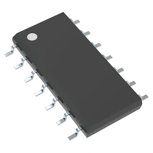
- Part No.:
- NLV14011BDR2G
- Manufacturer:
- onsemi
- Category:
- Gates and Inverters
- Package:
- 14-SOIC (0.154", 3.90mm Width)
- Datasheet:
-
 NLV14011BDR2G.pdf
- Description:
- IC GATE NAND 4CH 2-INP 14SOIC
- Quantity:
- Payment:

- Shipping:

Inventory:1,161
Please send an inquiry. Send us your inquiry, and we will respond immediately.
Product details
Overview
NLV14011BDR2G from onsemi is a quad 2-input NAND gate CMOS logic IC designed for low-power, high-noise-immunity digital control in automotive and industrial systems. It operates across 3.0–18.0 VDC supply, delivers ±4.2 mA output drive at 15 V, supports −55°C to +125°C ambient, and features triple diode input protection. It is used in engine control unit (ECU) signal conditioning and power management sequencing.
For engineers reviewing the NLV14011BDR2G datasheet, pinout, applications, or equivalent options, key selection criteria include wide-voltage operation, AEC-Q100 qualification, SOIC-14 packaging, and compatibility with legacy CD4000-series designs requiring automotive-grade reliability and ESD robustness (>3 kV HBM).
Technical Context
The NLV14011BDR2G implements four independent 2-input NAND gates using complementary MOS (CMOS) P- and N-channel enhancement-mode transistors in a monolithic structure. Each gate exhibits rail-to-rail output swing, buffered outputs, and guaranteed DC noise margins of 2.5 V at 15 VDD.
It uses standard B-series CMOS logic architecture with input thresholds defined by VIH/VIL ratios (e.g., VIH = 11 V, VIL = 4 V at VDD = 15 V), enabling interoperability with TTL loads and compatibility with mixed-voltage system interfaces across its full operating range.
Key Specifications
| Parameter | Value and Actual Design Meaning |
|---|---|
| Logic Function | Quad 2-input NAND - provides four independent Boolean AND-NOT operations per package |
| Supply Voltage Range | 3.0 V to 18.0 V - enables direct interface with 5 V, 12 V, and 15 V automotive/industrial rails without level shifting |
| Output Drive Current | ±4.2 mA at VDD = 15 V - sufficient to drive one low-power Schottky TTL load over full temperature range |
| Propagation Delay | 40 ns max at VDD = 15 V, CL = 50 pF - ensures timing predictability in synchronous control logic |
| Input Protection | Triple diode protection - enhances robustness against ESD and transient coupling in noisy under-hood environments |
| Operating Temperature | −55°C to +125°C - meets extended-range requirements for engine bay and powertrain applications |
| ESD Rating | >3000 V HBM - exceeds AEC-Q100 stress test requirements for human-body model |
Pinout & Package
Package: SOIC-14 (Case 751A-03), Pb-free, RoHS compliant, 8.55–8.75 mm × 3.80–4.00 mm footprint, 1.35–1.75 mm height.
| Pin/Terminal | Circuit Role | Design Meaning |
|---|---|---|
| 1, 2, 4, 5, 8, 9, 12, 13 | Input (IN1A–IN2D) | Eight total inputs - two per NAND gate; unused inputs must be tied to VDD or VSS to prevent floating states |
| 3, 6, 10, 11 | Output (OUTA–OUTD) | Four buffered logic outputs - each capable of sourcing/sinking up to ±4.2 mA at 15 V |
| 7 | VSS | Ground reference - all internal circuitry referenced to this node; must be low-impedance connection |
| 14 | VDD | Positive supply - powers all four gates; decoupling capacitor recommended near pin |
Key Features
| Feature | Design Value |
|---|---|
| AEC-Q100 Qualified | Qualified for automotive applications per Grade 1 (−40°C to +125°C) and Grade 3 (−40°C to +125°C) stress testing |
| Pb-Free & RoHS Compliant | Meets EU RoHS Directive 2011/65/EU and JESD204B; compatible with lead-free reflow profiles |
| Wide Supply Range | Operates from 3.0 V to 18.0 V - eliminates need for separate voltage regulators in multi-rail systems |
| High Noise Immunity | DC noise margin ≥2.5 V at 15 VDD - rejects common-mode interference in electrically harsh environments |
| Pin-for-Pin Compatible | Direct replacement for CD4011B and MC14011B - enables drop-in upgrade in legacy designs |
Applications
| Automotive Engine Control Unit (ECU) | Industrial PLC Input Conditioning |
|---|---|
Use Scenario: Signal inversion and enable logic for fuel injector drivers and camshaft position decoding. IC Role / Device Role / Timing Role: Quad NAND gate performs combinatorial logic for fault detection, mode selection, and pulse shaping. Use Value: Wide 3–18 V operation allows direct integration with 12 V battery-supplied ECU boards without LDOs. |
Use Scenario: Debouncing mechanical relay contacts and synchronizing discrete sensor inputs before ladder logic execution. IC Role / Device Role / Timing Role: Provides noise-filtered NAND-based gating for isolated digital inputs in modular I/O modules. Use Value: Triple diode input protection and >3 kV HBM rating ensure long-term reliability in factory-floor EMI environments. |
| Medical Infusion Pump Safety Logic | Renewable Energy Inverter Control |
Use Scenario: Dual-redundant interlock verification between motor enable signals and occlusion sensor status. IC Role / Device Role / Timing Role: Implements fail-safe NAND logic to block pump activation unless both safety conditions are met. Use Value: −55°C to +125°C operation supports sterilization cycles and extended field deployment in portable devices. |
Use Scenario: Gate-level logic for anti-islanding detection and DC-link precharge sequencing in solar inverters. IC Role / Device Role / Timing Role: Generates synchronized enable/disable pulses for IGBT gate drivers during soft-start transitions. Use Value: Buffered outputs drive multiple downstream logic stages while maintaining timing integrity across temperature extremes. |
Equivalent & Alternatives
The following parts are listed as comparable options for similar NAND gate applications.
| Alternative Part | Technical Difference | Application Difference | Selection Advice |
|---|---|---|---|
| MC14011BDR2G | Same logic function and pinout, but rated for −55°C to +125°C without AEC-Q100 qualification or PPAP support | Not qualified for automotive production; suitable for industrial or commercial prototypes | Select when AEC-Q100 compliance is not required and cost sensitivity outweighs automotive traceability needs |
| CD4011BM96 | Identical quad 2-input NAND function, but only rated to +85°C and lacks triple diode input protection | Limited to non-automotive, lower-reliability applications; no extended temperature or enhanced ESD capability | Choose for cost-sensitive consumer or educational designs where full automotive specs are unnecessary |
Compared with MC14011BDR2G and CD4011BM96, the NLV14011BDR2G uniquely combines AEC-Q100 qualification, triple-diode input protection, and full −55°C to +125°C operation - making it the only option qualified for safety-critical automotive powertrain control without derating or additional external protection.
Availability
NLV14011BDR2G is available at Aetrix Electronics and suitable for automotive ECU design, industrial PLC development, and medical device safety logic requiring stable component supply and long-term lifecycle assurance.
Supply support for NLV14011BDR2G includes scheduled delivery planning, volume procurement assistance, BOM continuity management, traceable sourcing, and lifecycle availability coordination for OEM customers, industrial embedded developers, connected-device designers, and electronics production programs.
Manufacturer
onsemi (formerly ON Semiconductor) is a global semiconductor manufacturer specializing in energy-efficient power, analog, sensing, and connectivity solutions for automotive, industrial, and cloud infrastructure markets.
The NLV14011BDR2G belongs to the B-Suffix Series CMOS Gates product line, engineered specifically for high-reliability, wide-voltage digital logic in automotive and harsh-environment applications where low power and noise immunity are critical.
FAQ
What is the maximum supply voltage rating for NLV14011BDR2G?
The NLV14011BDR2G has an absolute maximum DC supply voltage (VDD) rating of +18.0 V, with operational specification guaranteed from 3.0 V to 18.0 V. Exceeding 18.0 V may cause permanent damage, and operation below 3.0 V may result in undefined logic states or increased propagation delay. The NLV14011BDR2G maintains full functionality across this entire range, including at 12 V and 15 V automotive rails.
Is NLV14011BDR2G pin-compatible with CD4011B?
Yes, the NLV14011BDR2G is pin-for-pin compatible with CD4011B and other CD4000-series B-suffix devices. Its SOIC-14 pinout matches exactly: pins 1–2–4–5–8–9–12–13 are inputs, pins 3–6–10–11 are outputs, pin 7 is VSS, and pin 14 is VDD. This allows direct replacement in existing layouts without PCB modification, provided thermal and voltage margining align with NLV14011BDR2G's extended temperature and ESD specifications.
Does NLV14011BDR2G require external pull-up or pull-down resistors on unused inputs?
No - unused inputs on the NLV14011BDR2G must be tied directly to either VDD or VSS (not left floating), but external resistors are not required. Because it is a CMOS device with high-impedance inputs, connecting unused inputs to a valid logic rail via a direct trace or short ensures stable operation and prevents oscillation or excessive current draw. The NLV14011BDR2G does not incorporate internal termination resistors.
What is the output drive capability of NLV14011BDR2G at 5 V supply?
At VDD = 5.0 V, the NLV14011BDR2G guarantees a minimum sink current (IOL) of 0.64 mA and source current (IOH) of −0.64 mA while maintaining VOL ≤ 0.05 V and VOH ≥ 4.95 V. This is sufficient to drive two low-power TTL loads, supporting interoperability with legacy 5 V logic families without level translators. The NLV14011BDR2G maintains these values across −55°C to +125°C ambient.
How does the triple diode input protection on NLV14011BDR2G differ from standard double diode protection?
The NLV14011BDR2G features triple diode input protection - two clamping diodes to VDD and VSS plus a third series diode - enhancing transient suppression beyond standard double-diode schemes. This configuration improves resilience against fast-rising ESD events and inductive kickback in automotive harnesses. Unlike standard double-diode protection found on most MC14001B-series parts, this feature is explicitly specified for NLV14011BDR2G and NLV14081B variants per the datasheet.
NLV14011BDR2G Specifications
- Product attributes
- Attribute value
- Manufacturer:
- onsemi
- Series:
- 4000B
- Package/Case:
- 14-SOIC (0.154", 3.90mm Width)
- Packaging:
- Tape & Reel (TR)
- Product Status:
- Active
- Logic Type:
- NAND Gate
- Number of Circuits:
- 4
- Number of Inputs:
- 2
- Features:
- -
- Voltage - Supply:
- 3V ~ 18V
- Current - Quiescent (Max):
- 1 µA
- Current - Output High, Low:
- 8.8mA, 8.8mA
- Input Logic Level - Low:
- 1.5V ~ 4V
- Input Logic Level - High:
- 3.5V ~ 11V
- Max Propagation Delay @ V, Max CL:
- 80ns @ 15V, 50pF
- Operating Temperature:
- -55°C ~ 125°C
- Grade:
- -
- Qualification:
- -
- Mounting Type:
- Surface Mount
- Supplier Device Package:
- 14-SOIC
NLV14011BDR2G FAQ
1.How can I place an order for NLV14011BDR2G through Aetrix?
Please submit a Request for Quotation (RFQ) for NLV14011BDR2G on Aetrix. Our sales agent will provide a competitive quotation and guide you through the order confirmation once you accept the terms.
2.Are the price and stock information for NLV14011BDR2G reliable?
The price and inventory of NLV14011BDR2G are updated periodically and may fluctuate due to market conditions. Stock and pricing data are typically refreshed every 24 hours. Quotation validity for NLV14011BDR2G is usually 5 days.
3.What payment methods are accepted for NLV14011BDR2G?
We accept Wire Transfer, PayPal, Credit Card, Western Union, MoneyGram, and Escrow for NLV14011BDR2G transactions.
Note: Certain payment methods may incur a processing fee.
4.How is shipping managed for NLV14011BDR2G?
NLV14011BDR2G orders can be shipped via leading logistics carriers, including DHL, UPS, FedEx, TNT, or Registered Mail.
Once your NLV14011BDR2G order is processed, you will receive an email with the shipment details and tracking number.
Note: Tracking information may take up to 24 hours to appear. Express delivery typically takes 3–5 business days.
5.How can I obtain technical support or documentation for NLV14011BDR2G?
For technical support, including NLV14011BDR2G datasheets, pinout diagrams, or application guidance, please contact our engineering support team. They can provide detailed documentation and assistance for your NLV14011BDR2G requirements.
6.How does Aetrix verify that NLV14011BDR2G is sourced from the original manufacturer or authorized distributors?
All NLV14011BDR2G products on Aetrix are procured from qualified distributors and authorized channels. Our dedicated quality assurance team conducts strict verification, including traceability checks and, if necessary, third-party testing. This ensures that NLV14011BDR2G meets industry standards.
7.What is the process for return or replacement of NLV14011BDR2G?
All NLV14011BDR2G units undergo pre-shipment inspection (PSI). If there is an issue with NLV14011BDR2G, returns or replacements are accepted under the following conditions:
1.Quantity discrepancies, incorrect items, or visible external defects (such as breakage or corrosion), acknowledged by Aetrix.
2.The issue is reported within 90 days of delivery.
3.The NLV14011BDR2G part is unused and in its original packaging.
Return procedure for NLV14011BDR2G:
1.Submit a request within 90 days.
2.Obtain a Return Material Authorization (RMA) from Aetrix.
NLV14011BDR2G Tags

-
SN74LVC1G14DBVR
Texas Instruments

-
SN74LVC1G14DCKR
Texas Instruments
-
SN74AHC1G14DBVR
Texas Instruments
-
SN74LVC1G08DBVR
Texas Instruments
-
SN74LVC1G08DCKR
Texas Instruments
-
SN74LVC1G32DCKR
Texas Instruments
-
SN74LVC1G04DBVR
Texas Instruments
.jpg)
-
74LVC1G08GW,125
Nexperia USA Inc.
-
SN74LVC1G04DCKR
Texas Instruments
-
SN74AHC1G08DBVR
Texas Instruments
-
SN74LVC1G32DBVR
Texas Instruments
-
SN74AHCT1G08DBVR
Texas Instruments
Tech Hub

Counterfeit components can hide behind convincing markings and passing basic function tests. This engineering reference covers source traceability, external inspection, X-ray, XRF, electrical testing, …

A practical engineering and sourcing framework covering lifecycle verification, lifetime-buy calculations, replacement qualification, supplier checks and counterfeit-risk controls.

TTL and CMOS logic families differ in thresholds, loading, output drive, power and timing. This engineering guide compares 74HC and 74HCT, calculates noise margins and checks 3.3 V/5 V compatibility.

A practical engineering guide to 3.3V and 5V logic compatibility, input thresholds, resistor dividers, translator ICs, MOSFET level shifting, I2C pull-ups, timing limits and power-sequencing risks.

The 74HC595 uses push-pull logic outputs, while the TPIC6B595 uses 50 V open-drain DMOS sinks for higher-power loads. This guide compares timing, current limits, 3.3 V interfacing, load wiring, thermal…

The 74HC595 converts serial data into eight stable parallel outputs. This guide covers pin functions, shift and storage timing, OE and MR behavior, drive-current limits, cascading, voltage compatibilit…

A technical comparison of level-sensitive latches and edge-triggered flip-flops, covering timing windows, setup and hold limits, master–slave operation, time borrowing, race-through, HDL inference and…

A D latch stores one bit while Enable controls when data can pass. This reference covers gate-level operation, truth tables, transparency, setup and hold timing, LE versus OE, common ICs and practical …

An SR latch stores one bit through cross-coupled feedback. This engineering reference covers NOR and NAND implementations, truth tables, forbidden-state recovery, gated operation, switch debouncing, fa…

Latch circuits retain one bit through feedback. This technical reference covers SR and D latches, truth tables, transparency, timing limits, latch-versus-flip-flop behavior, applications and common log…


