
 My Inquiry
 My Account


Texas Instruments NS486SXF-25/NOPB
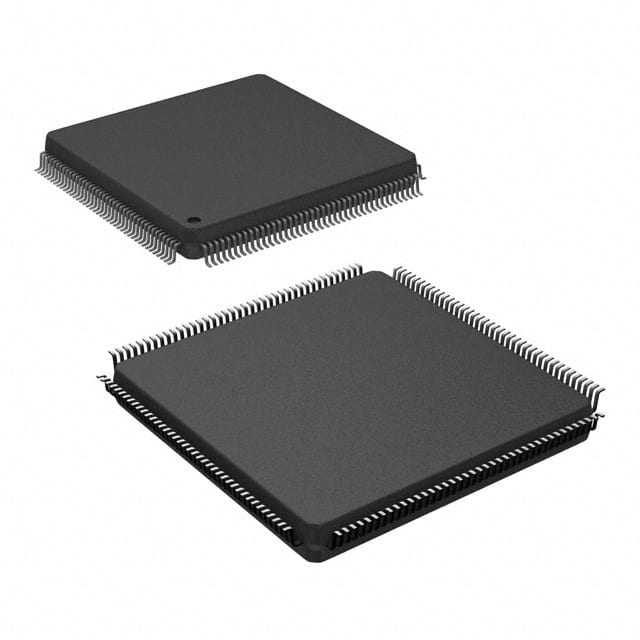
- Part No.:
- NS486SXF-25/NOPB
- Manufacturer:
- Texas Instruments
- Category:
- Microprocessors
- Package:
- 160-BFQFP
- Datasheet:
-
 NS486SXF-25/NOPB.pdf
- Description:
- IC MPU INTEL486 SX 25MHZ 160QFP
- Quantity:
- Payment:

- Shipping:

Inventory:3,302
Please send an inquiry. Send us your inquiry, and we will respond immediately.
Product details
Overview
NS486SXF-25/NOPB from National Semiconductor is a 32-bit embedded system controller integrating an Intel486-class protected-mode CPU core, on-chip DRAM controller (supporting up to 16 MB total), six-channel DMA, IEEE 1284 ECP parallel port, PCMCIA 2.0 interface, UART with IrDA v1.0, LCD controller (480×320), and reconfigurable I/O - all in a single 160-pin PQFP package operating at 25 MHz on 5 V. It targets fax machines, multifunction peripherals, set-top boxes, and mobile communicators.
For engineers reviewing the NS486SXF-25/NOPB datasheet, NS486SXF-25/NOPB pinout, NS486SXF-25/NOPB application, or NS486SXF-25/NOPB equivalent, key selection considerations include its 25 MHz 5V operation, glueless ISA-compatible bus, protected-mode-only 486 instruction set, integrated real-time clock/calendar, and programmable power management for battery-operated embedded systems.
Technical Context
The NS486SXF-25/NOPB implements a RISC-optimized 32-bit processor core executing Intel486 protected-mode instructions with a 1 KB instruction cache and three-stage pipeline - no real mode, virtual memory, or FPU support. It boots directly into protected mode and uses a 50 MHz crystal divided by two for its 25 MHz CPU clock.
Its system service elements include a dual-bank DRAM controller (page-mode, up to 8 MB per bank), six-channel DMA (four external, two internal to ECP/LCD), dual cascaded 8259-compatible interrupt controllers (15 IRQs), 1 kHz protected WATCHDOG timer (CH2), and DS1287-compatible RTC with 50-byte CMOS RAM and alarm functions.
Key Specifications
| Parameter | Value and Actual Design Meaning |
|---|---|
| CPU Core | Intel486-class, protected-mode only; boots directly into protected mode - eliminates real-mode initialization overhead and reduces silicon area. |
| Operating Frequency | 25 MHz at 5 V ±5%; derived from 50 MHz crystal via on-chip divide-by-2 - simplifies clock sourcing and reduces external component count. |
| DRAM Support | Two banks, up to 8 MB each; page-mode read/write; programmable CAS-before-RAS refresh - enables fast contiguous data access without external cache. |
| DMA Channels | Six total: four external (25 MB/s max @ 25 MHz), two internal (to ECP port and LCD controller) - offloads high-bandwidth transfers from CPU for real-time display and printing. |
| Parallel Interface | IEEE 1284 ECP mode with Host/Slave capability - supports bidirectional high-speed peripheral control (e.g., printers, scanners) without external logic. |
| LCD Controller | Supports 480×320 monochrome grayscale displays with DRAM-based frame buffer and 60–90 Hz refresh - enables embedded GUIs with minimal external video components. |
| Power Management | CPU clock division (÷4, ÷8, ÷16, ÷32, ÷64), per-peripheral clock gating, and idle-mode CPU clock disable - achieves granular power control for portable and low-power systems. |
Pinout & Package
The NS486SXF-25/NOPB is housed in a 160-pin Plastic Quad Flat Package (PQFP) compliant with JEDEC MS-026, measuring 28 mm × 28 mm with 0.65 mm lead pitch. Thermal and mechanical data align with National Semiconductor's standard PQFP specifications for embedded industrial use.
| Pin/Terminal | Circuit Role | Design Meaning |
|---|---|---|
| SA[25:0] | System Address Bus | 26-bit multiplexed address output; carries latched CPU address or cascaded interrupt vectors; SA[0] sampled at reset to select ICE mode. |
| SD[15:0] | System Data Bus | 16-bit bidirectional data path; upper byte (SD[15:8]) unused during 8-bit transfers - supports mixed 8/16-bit peripheral interfacing. |
| SBHE | Byte High Enable | Active-low signal indicating high-byte transfer on SD[15:8]; sampled at power-on to detect boot ROM width - enables automatic 8/16-bit memory configuration. |
| IOR / IOW | I/O Read/Write Control | Active-low strobes for I/O-mapped transactions; compatible with ISA timing - allows direct connection to legacy ISA peripherals without glue logic. |
| MEMR / MEMW | Memory Read/Write Control | Active-low strobes for memory-mapped accesses; synchronized with SA/SD - supports external SRAM, Flash, and DRAM with wait-state insertion via RDY. |
| RDY | Wait-State Input | Open-collector or tri-state input to extend bus cycles; driven low by slow peripherals - enables flexible timing adaptation without CPU modification. |
Key Features
| Feature | Design Value |
|---|---|
| Reconfigurable I/O | Up to 29 pins dynamically reassigned as general-purpose bidirectional I/O when UART, ECP, LCD, or PCMCIA functions are disabled - maximizes pin utility across product variants. |
| PCMCIA Interface | Single-slot PCMCIA 2.0 support with ExCA 1.50 and XIP capability - enables hot-pluggable storage and modem expansion with minimal external circuitry. |
| IrDA v1.0 UART | NS16550-compatible serial port with 16-byte FIFO and HP-SIR infrared mode - delivers reliable wireless data exchange at up to 115.2 kbps without external transceivers. |
| WATCHDOG Timer | Protected 16-bit CH2 timer driven by 1 kHz RTC clock; generates reset/interrupt on timeout - ensures deterministic recovery from firmware hangs in unattended systems. |
| MICROWIRE/Access.bus | Configurable 2-wire (Access.bus) or 3-wire (MICROWIRE/SPI-phase) serial interface - simplifies connection to EEPROMs, A/D converters, and clock chips using industry-standard protocols. |
Applications
| Fax Machine Control | Multifunction Peripheral (MFP) |
|---|---|
Use Scenario: Integrated fax engine managing document scanning, compression, modem transmission, and thermal printing. IC Role / Device Role / Timing Role: Central controller executing real-time OS (VRTX/pSOSa), coordinating DRAM-buffered image processing, PCMCIA-based firmware updates, and IrDA-linked status reporting. Use Value: Single-chip integration eliminates discrete DMA, UART, and timer ICs; ECP port drives printer engine directly; 25 MHz performance sustains G3 fax throughput. | Use Scenario: Shared platform for scanner, copier, and printer functions with interchangeable firmware and modular hardware. IC Role / Device Role / Timing Role: System-on-chip host managing concurrent LCD UI, USB/ECP peripheral arbitration, DRAM-based scan buffer, and RTC-scheduled tasks. Use Value: Reconfigurable I/O adapts pinout to module presence; LCD controller drives 320×240 panel natively; nine chip selects enable flexible peripheral expansion. |
| Set-Top Box (STB) | Mobile Communicator |
Use Scenario: Digital TV receiver decoding MPEG-2 streams, rendering OSD menus, and handling IR remote input. IC Role / Device Role / Timing Role: Protected-mode kernel host running QNX Neutrino; DRAM controller buffers video frames; UART handles IR demodulation and debug console. Use Value: 1 KB instruction cache improves code fetch efficiency from Flash; power management modes reduce standby current; RTC maintains EPG time. | Use Scenario: Handheld organizer with PDA functionality, SMS messaging, and infrared file exchange. IC Role / Device Role / Timing Role: Real-time executive host (VxWorks) managing LCD refresh, IrDA v1.0 comms, battery-backed RTC alarms, and PCMCIA modem card. Use Value: Integrated IrDA PHY eliminates external transceiver; 29 reconfigurable I/O pins support custom keypad and sensor interfaces; low-power idle modes extend battery life. |
Equivalent & Alternatives
The following parts are listed as comparable options for similar embedded controller applications.
| Alternative Part | Technical Difference | Application Difference | Selection Advice |
|---|---|---|---|
| AMD ÉLAN SC400-25 | 25 MHz x86-compatible core with integrated PCI, USB 1.1, and enhanced power management; larger die, different pinout. | Targets higher-integration designs requiring USB connectivity and PCI expansion - not drop-in compatible. | Select for new designs needing USB/PCI; avoid for NS486SXF-25/NOPB footprint or software migration. |
| Intel 386EX C33 | 33 MHz 386SX core with integrated timers, UART, and watchdog; no ECP port, LCD controller, or PCMCIA; 132-pin LQFP. | Suitable for simpler control applications without graphics or high-speed parallel I/O - lower gate count and cost. | Choose when LCD/ECP/PCMCIA are unnecessary and legacy 386 toolchains are preferred. |
Compared with AMD ÉLAN SC400-25 and Intel 386EX C33, the NS486SXF-25/NOPB uniquely combines 486-class performance with integrated ECP, LCD, and PCMCIA in a 160-pin PQFP - making it optimal for cost-sensitive, graphics-capable embedded systems where those peripherals are essential.
Availability
NS486SXF-25/NOPB is available at Aetrix Electronics and suitable for fax machines, multifunction peripherals, set-top boxes, and mobile communicators requiring stable component supply across long-lifecycle embedded programs.
Supply support for NS486SXF-25/NOPB includes scheduled delivery planning, volume procurement assistance, BOM continuity management, traceable sourcing, and lifecycle availability coordination for OEM customers, industrial embedded developers, connected-device designers, and electronics production programs.
Manufacturer
National Semiconductor was a U.S.-based semiconductor company specializing in analog, interface, and embedded controller solutions before its acquisition by Texas Instruments in 2011.
The NS486SXF product line was designed as a highly integrated, cost-optimized 486-class embedded controller targeting office automation and communication devices - emphasizing glueless ISA compatibility, power efficiency, and peripheral consolidation.
FAQ
What is the maximum DRAM capacity supported by the NS486SXF-25/NOPB?
The NS486SXF-25/NOPB supports up to 16 MB of DRAM total: two independently configurable banks, each up to 8 MB. Each bank uses a 16-bit data path and supports page-mode operations with programmable CAS latency and refresh timing. Parity support requires 18-bit-wide DRAMs when enabled.
Does the NS486SXF-25/NOPB support real-mode x86 execution?
No, the NS486SXF-25/NOPB operates exclusively in protected mode and does not support real-mode or virtual 8086 mode. Its processor core omits real-mode initialization logic, floating-point unit interface, and virtual memory paging - optimizations that reduce die size and power consumption for embedded RTOS environments like VxWorks and QNX Neutrino.
Can the NS486SXF-25/NOPB drive a color LCD display?
No, the NS486SXF-25/NOPB LCD controller is limited to monochrome supertwist displays with up to 4 gray levels (1- or 2-bit per pixel). It supports resolutions including 320×240, 320×200, and 480×320 but lacks hardware acceleration, RGB interface, or color palette registers required for color TFT or STN panels.
How many interrupt sources does the NS486SXF-25/NOPB provide?
The NS486SXF-25/NOPB provides 15 programmable interrupt sources via two cascaded 8259A-compatible interrupt controllers. Three IRQs are reserved for RTC tick, RTC alarm, and cascade channel; the remaining 12 are available for internal peripherals (UART, timers, ECP) or external devices connected to the ISA-like bus.
Is the NS486SXF-25/NOPB pin-compatible with the NS486TMSXF variant?
Yes, the NS486SXF-25/NOPB and NS486TMSXF share identical 160-pin PQFP packaging, pinout, and electrical characteristics. The TMSXF variant adds temperature monitoring circuitry but maintains full functional and mechanical compatibility - allowing direct substitution in thermally constrained industrial applications without PCB changes.
NS486SXF-25/NOPB Specifications
- Product attributes
- Attribute value
- Manufacturer:
- Texas Instruments
- Package/Case:
- 160-BFQFP
- Series:
- -
- Packaging:
- Tray
- Product Status:
- Active
- Core Processor:
- Intel486 SX
- Number of Cores/Bus Width:
- 1 Core, 32-Bit
- Speed:
- 25MHz
- Co-Processors/DSP:
- -
- RAM Controllers:
- DRAM
- Graphics Acceleration:
- No
- Display & Interface Controllers:
- LCD
- Ethernet:
- -
- SATA:
- -
- USB:
- -
- Voltage - I/O:
- 3.3V, 5.0V
- Operating Temperature:
- 0°C ~ 70°C (TA)
- Grade:
- -
- Qualification:
- -
- Security Features:
- -
- Mounting Type:
- Surface Mount
- Supplier Device Package:
- 160-QFP (28x28)
- Additional Interfaces:
- Access.bus, IrDA, Microwire, PCMCIA, UART
NS486SXF-25/NOPB FAQ
1.How can I place an order for NS486SXF-25/NOPB through Aetrix?
Please submit a Request for Quotation (RFQ) for NS486SXF-25/NOPB on Aetrix. Our sales agent will provide a competitive quotation and guide you through the order confirmation once you accept the terms.
2.Are the price and stock information for NS486SXF-25/NOPB reliable?
The price and inventory of NS486SXF-25/NOPB are updated periodically and may fluctuate due to market conditions. Stock and pricing data are typically refreshed every 24 hours. Quotation validity for NS486SXF-25/NOPB is usually 5 days.
3.What payment methods are accepted for NS486SXF-25/NOPB?
We accept Wire Transfer, PayPal, Credit Card, Western Union, MoneyGram, and Escrow for NS486SXF-25/NOPB transactions.
Note: Certain payment methods may incur a processing fee.
4.How is shipping managed for NS486SXF-25/NOPB?
NS486SXF-25/NOPB orders can be shipped via leading logistics carriers, including DHL, UPS, FedEx, TNT, or Registered Mail.
Once your NS486SXF-25/NOPB order is processed, you will receive an email with the shipment details and tracking number.
Note: Tracking information may take up to 24 hours to appear. Express delivery typically takes 3–5 business days.
5.How can I obtain technical support or documentation for NS486SXF-25/NOPB?
For technical support, including NS486SXF-25/NOPB datasheets, pinout diagrams, or application guidance, please contact our engineering support team. They can provide detailed documentation and assistance for your NS486SXF-25/NOPB requirements.
6.How does Aetrix verify that NS486SXF-25/NOPB is sourced from the original manufacturer or authorized distributors?
All NS486SXF-25/NOPB products on Aetrix are procured from qualified distributors and authorized channels. Our dedicated quality assurance team conducts strict verification, including traceability checks and, if necessary, third-party testing. This ensures that NS486SXF-25/NOPB meets industry standards.
7.What is the process for return or replacement of NS486SXF-25/NOPB?
All NS486SXF-25/NOPB units undergo pre-shipment inspection (PSI). If there is an issue with NS486SXF-25/NOPB, returns or replacements are accepted under the following conditions:
1.Quantity discrepancies, incorrect items, or visible external defects (such as breakage or corrosion), acknowledged by Aetrix.
2.The issue is reported within 90 days of delivery.
3.The NS486SXF-25/NOPB part is unused and in its original packaging.
Return procedure for NS486SXF-25/NOPB:
1.Submit a request within 90 days.
2.Obtain a Return Material Authorization (RMA) from Aetrix.
NS486SXF-25/NOPB Tags

-
AT91SAM9260B-CU-999
Microchip Technology
-
AT91SAM9G25-CU
Microchip Technology

-
ATSAMA5D27C-CU
Microchip Technology
-
AT91SAM9X35-CU
Microchip Technology
-
AT91SAM9X25-CU
Microchip Technology

-
MCIMX6Y2CVM08AB
NXP Semiconductors
.JPG)
-
AM3352BZCZ100
Texas Instruments
-
AT91SAM9260B-CU
Microchip Technology

-
AT91SAM9260B-QU
Microchip Technology

-
ATSAMA5D31A-CU
Microchip Technology
-
AT91SAM9G20B-CU-999
Microchip Technology
-
MCIMX6Y2CVM05AB
NXP Semiconductors
Tech Hub

A practical engineering guide to 3.3V and 5V logic compatibility, input thresholds, resistor dividers, translator ICs, MOSFET level shifting, I2C pull-ups, timing limits and power-sequencing risks.

The 74HC595 uses push-pull logic outputs, while the TPIC6B595 uses 50 V open-drain DMOS sinks for higher-power loads. This guide compares timing, current limits, 3.3 V interfacing, load wiring, thermal…

The 74HC595 converts serial data into eight stable parallel outputs. This guide covers pin functions, shift and storage timing, OE and MR behavior, drive-current limits, cascading, voltage compatibilit…

A technical comparison of level-sensitive latches and edge-triggered flip-flops, covering timing windows, setup and hold limits, master–slave operation, time borrowing, race-through, HDL inference and…

A D latch stores one bit while Enable controls when data can pass. This reference covers gate-level operation, truth tables, transparency, setup and hold timing, LE versus OE, common ICs and practical …

An SR latch stores one bit through cross-coupled feedback. This engineering reference covers NOR and NAND implementations, truth tables, forbidden-state recovery, gated operation, switch debouncing, fa…

Latch circuits retain one bit through feedback. This technical reference covers SR and D latches, truth tables, transparency, timing limits, latch-versus-flip-flop behavior, applications and common log…

An engineering guide to LED driver operation, constant-current and constant-voltage outputs, linear and switching topologies, dimming, IC selection, calculations, replacement compatibility, and fault c…

Operational amplifier guide covering op amp basics, feedback, ideal vs real op amps, common configurations, buffer circuits, offset, bias current, gain-bandwidth, slew rate, rail-to-rail limits and sel…

Jumper cables guide covering safe connection order, red and black clamp placement, final ground connection, cable gauge, length, clamp quality, copper vs CCA cables, jump starter comparison and battery…


