
 My Inquiry
 My Account


onsemi NUS3045MNT1G
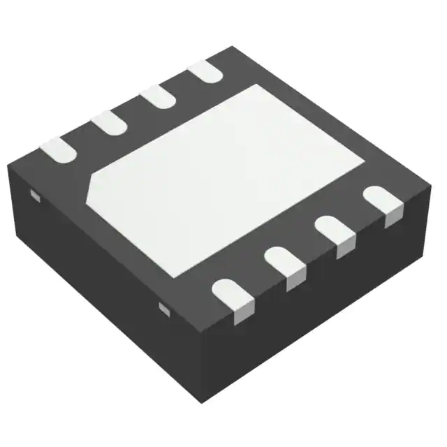
- Part No.:
- NUS3045MNT1G
- Manufacturer:
- onsemi
- Category:
- Mixed Technology
- Package:
- 8-VDFN Exposed Pad
- Datasheet:
-
 NUS3045MNT1G.pdf
- Description:
- TVS DEVICE MIXED 7.08V 8-DFN
- Quantity:
- Payment:

- Shipping:

Inventory:3,490
Please send an inquiry. Send us your inquiry, and we will respond immediately.
Product details
Overview
NUS3045MNT1G from onsemi is an overvoltage protection IC with integrated −30 V P-channel power MOSFET, designed for input-side fault protection in portable electronics powered by AC-DC adapters or car chargers. It features a nominal 6.85 V overvoltage threshold, 2.8 V undervoltage lockout, 66 mΩ RDS(on) at −4.5 V, <1.0 µs turn-off delay, and operates across −40°C to +85°C ambient.
For engineers reviewing the NUS3045MNT1G datasheet, pinout, applications, or equivalent options, this page delivers verified electrical parameters, DFN8 package layout, real-world use cases in Li-ion battery-powered systems, and validated alternative parts for supply continuity and design flexibility.
Technical Context
The NUS3045MNT1G integrates an NCP345-based OVP controller with a monolithically co-packaged −30 V P-channel MOSFET. Its dual-input protection logic responds independently to overvoltage events on the IN pin (threshold = 6.85 V ±100 mV) and logic-level CNTRL signals (1.5 V high, 0.5 V low), enabling both automatic fault shutdown and manual system control.
It implements fast gate drive with <1.0 µs overvoltage turn-off time (CL ≤ 12 nF), undervoltage lockout at 2.8 V (±0.2 V), and supports 1.8 V–5.0 V logic-compatible control inputs. The integrated FET delivers 66 mΩ RDS(on) at −4.5 V and −1.0 A continuous drain current, with thermal resistance of 104.3°C/W (junction-to-air).
Key Specifications
| Parameter | Value and Actual Design Meaning |
|---|---|
| Overvoltage Threshold | 6.85 V nominal; triggers disconnect within 1.0 µs when input exceeds this level, protecting downstream Li-ion cells or PMICs. |
| Undervoltage Lockout | 2.8 V nominal; disables output when VCC drops below this, preventing erratic behavior during brownout or weak adapter conditions. |
| RDS(on) | 66 mΩ at −4.5 V; enables low conduction loss for 1.0 A load current, minimizing heat rise in compact DFN8 footprint. |
| Turn-off Delay (IN) | ≤1.0 µs (typical 0.5 µs); ensures sub-microsecond response to overvoltage transients, meeting IEC 61000-4-5 surge immunity timing requirements. |
| Control Input Logic Level | Compatible with 1.8 V CMOS; allows direct interface to low-voltage microcontrollers without level-shifting circuitry. |
| Package | 3.3 × 3.3 mm DFN8 (Case 506AL); Pb-free, reflow-rated to 260°C, optimized for space-constrained portable PCB layouts. |
| Operating Temperature | −40°C to +85°C ambient; validated for use in smartphones, digital cameras, and automotive accessory chargers. |
Pinout & Package
Package: 3.3 mm × 3.3 mm, 0.9 mm height, 8-pin DFN (Case 506AL), exposed thermal pad, Pb-free (MNT1G suffix), JEDEC-compliant reflow profile (260°C peak).
| Pin/Terminal | Circuit Role | Design Meaning |
|---|---|---|
| 1 (IN) | Overvoltage sense input | Monitors input rail voltage; initiates FET disconnect when >6.85 V; supports external resistor scaling for higher thresholds. |
| 2,10 (GND) | Power and signal ground reference | Common return path for OVP logic, gate driver, and FET source; must be low-impedance connection to minimize noise coupling. |
| 3 (CNTRL) | Logic enable/disable input | Active-high control: logic high forces OUT high → FET off; floating or unconnected requires tie-to-GND for default operation. |
| 4,9 (DRAIN) | Power MOSFET drain terminal | Connects to input supply (e.g., adapter output); carries full load current and absorbs transient energy during fault events. |
| 5 (SRC) | Power MOSFET source terminal | Connects to load side (e.g., battery charger IC input); forms high-side switch configuration with DRAIN as input node. |
| 6 (GATE) | MOSFET gate drive output | Driven internally by OVP logic; not user-accessible - internal connection only; no external gate resistor required. |
| 7 (OUT) | Gate driver output signal | Drives MOSFET gate to VCC − 1.0 V (high) or GND (low); slew rate and drive strength optimized for <12 nF total gate capacitance. |
| 8 (VCC) | Supply voltage input | Power for OVP circuitry; derived from input rail via internal regulator; shuts down if voltage falls below 2.8 V. |
Key Features
| Feature | Design Value |
|---|---|
| Integrated −30 V P-channel MOSFET | Eliminates need for discrete FET and driver, reducing BOM count by ≥3 components and saving ≥4 mm² PCB area. |
| Accurate 6.85 V overvoltage threshold | Matches single-cell Li-ion maximum charge voltage (4.2 V × 1.63 = ~6.85 V), enabling precise battery-side overvoltage cutoff without calibration. |
| Sub-1 µs fault response time | Prevents >10 V transients from reaching sensitive load ICs (e.g., USB PD controllers or battery fuel gauges) before damage occurs. |
| 1.8 V logic-compatible CNTRL input | Directly interfaces with modern ultra-low-power MCUs (e.g., ARM Cortex-M0+) without level shifters or pull-up resistors. |
| Low 66 mΩ RDS(on) at −4.5 V | Limits conduction loss to <300 mW at 1.0 A, avoiding thermal derating in sealed handheld enclosures. |
Applications
| Smartphone Charging Protection | Digital Camera Power Management |
|---|---|
|
Use Scenario: AC adapter or car charger supplies power to smartphone mainboard during charging, subject to line surges and adapter faults. IC Role / Device Role / Timing Role: High-side overvoltage protector placed between adapter input and USB-C port controller/battery charger IC. Use Value: Disables power path in <1.0 µs upon >6.85 V detection, preventing latch-up or oxide breakdown in 28 nm/16 nm PMICs. |
Use Scenario: External power supply powers image sensor, ISP, and flash LED drivers in DSLR/mirrorless cameras. IC Role / Device Role / Timing Role: Input rail supervisor ensuring stable 5 V or 3.3 V supply to high-speed serial interfaces (e.g., MIPI CSI-2). Use Value: Blocks overvoltage before it corrupts sensor data streams or damages flash capacitor charging circuits. |
| Portable Medical Monitor | Bluetooth Headset Battery Charging |
|
Use Scenario: Rechargeable Li-ion battery in handheld ECG or pulse oximeter powered via USB wall adapter. IC Role / Device Role / Timing Role: Primary overvoltage barrier between adapter and battery protection IC (e.g., BQ297xx series). Use Value: Prevents overcharge-induced thermal runaway by cutting off >6.85 V before battery management IC enters fault mode. |
Use Scenario: Micro-USB or USB-C input to compact wireless headset charging circuit with integrated Li-ion cell. IC Role / Device Role / Timing Role: Input-stage protector upstream of linear charger IC (e.g., MCP73831) and LDO regulators. Use Value: Enables safe hot-plug operation with legacy chargers while maintaining <100 µA quiescent current during standby. |
Equivalent & Alternatives
The following parts are listed as comparable options for similar overvoltage protection applications.
| Alternative Part | Technical Difference | Application Difference | Selection Advice |
|---|---|---|---|
| TPS259210DRCT | −20 V rating, 40 mΩ RDS(on), integrated current limiting, but no undervoltage lockout or 1.8 V CNTRL support. | Best suited for 5 V USB-powered systems requiring foldback current limiting; less suitable for 3.7 V Li-ion adapter inputs. | Select when precise current limiting and lower RDS(on) outweigh need for UVLO and wide logic compatibility. |
| NCP345MUTBG | Standalone OVP controller (no integrated FET); requires external −30 V P-MOSFET; identical 6.85 V threshold and 1.8 V CNTRL. | Used where board space allows discrete FET placement and thermal design requires separate FET die attach. | Choose when thermal management demands separation of control logic and power switching elements. |
Compared with NUS3045MNT1G, TPS259210DRCT offers lower conduction loss but lacks UVLO and 1.8 V logic support, while NCP345MUTBG provides identical protection logic but requires external FET layout and thermal design effort.
Availability
NUS3045MNT1G is available at Aetrix Electronics and suitable for smartphone charging protection, digital camera power management, portable medical monitors, Bluetooth headset battery charging, and other applications requiring stable component supply with guaranteed long-term sourcing.
Supply support for NUS3045MNT1G includes scheduled delivery planning, volume procurement assistance, BOM continuity management, traceable sourcing, and lifecycle availability coordination for OEM customers, industrial embedded developers, connected-device designers, and electronics production programs.
Manufacturer
onsemi (formerly ON Semiconductor) is a global semiconductor supplier focused on energy-efficient innovation for automotive, industrial, cloud, and IoT applications.
The NUS3045MNT1G belongs to onsemi's Overvoltage Protection IC product line, engineered specifically to simplify robust input-stage protection in space- and cost-constrained portable electronics using Li-ion batteries.
FAQ
What is the overvoltage threshold accuracy of the NUS3045MNT1G?
The NUS3045MNT1G has a nominal overvoltage threshold of 6.85 V, with a specified tolerance of ±100 mV (6.65 V to 7.08 V) at 25°C. This accuracy is maintained across −40°C to +85°C ambient temperature, as confirmed by Figure 2 in the official datasheet. The NUS3045MNT1G uses trimmed internal references to ensure consistent trip points without external calibration.
Can the NUS3045MNT1G be used with a 5 V input supply?
Yes, the NUS3045MNT1G supports VCC operating voltages from 3.0 V to 25 V, making it fully compatible with 5 V adapter inputs. Its 6.85 V overvoltage threshold ensures safe operation under normal 5 V conditions while still protecting against accidental 9 V or 12 V misconnections. The NUS3045MNT1G also includes undervoltage lockout at 2.8 V, preventing false triggering during startup or brownout.
Does the NUS3045MNT1G require an external gate resistor?
No, the NUS3045MNT1G does not require an external gate resistor. Its internal gate driver is optimized for direct connection to the integrated −30 V P-channel MOSFET, with drive strength calibrated for ≤12 nF total gate capacitance. Adding an external resistor would degrade the <1.0 µs turn-off response time and is explicitly discouraged in the datasheet's application circuits.
How does the CNTRL pin function in the NUS3045MNT1G?
The CNTRL pin on the NUS3045MNT1G is an active-high logic input that overrides overvoltage detection: logic high (≥1.5 V) forces the OUT pin high, turning off the internal FET regardless of IN voltage; logic low (≤0.5 V) enables normal OVP operation. If unused, CNTRL must be tied to GND. This feature allows host MCU firmware to disable power during sleep or fault recovery - a capability built into the NUS3045MNT1G's core architecture.
What is the thermal performance of the NUS3045MNT1G in a typical PCB layout?
The NUS3045MNT1G has a junction-to-air thermal resistance (RθJA) of 104.3°C/W when mounted on a standard FR4 board with a 1-inch² copper pad (1 oz Cu). At 1.0 A load current and 66 mΩ RDS(on), power dissipation is ~66 mW, resulting in <7°C junction-to-ambient rise - well within its 150°C max junction rating. This thermal margin is validated in the datasheet's maximum ratings table and supports continuous operation in sealed portable enclosures.
NUS3045MNT1G Specifications
- Product attributes
- Attribute value
- Manufacturer:
- onsemi
- Package/Case:
- 8-VDFN Exposed Pad
- Series:
- -
- Packaging:
- Tape & Reel (TR)
- Product Status:
- Obsolete
- Voltage - Clamping:
- 7.08V
- Technology:
- Mixed Technology
- Number of Circuits:
- 1
- Applications:
- General Purpose
- Grade:
- -
- Qualification:
- -
- Mounting Type:
- Surface Mount
- Supplier Device Package:
- 8-DFN (3.3x3.3)
NUS3045MNT1G FAQ
1.How can I place an order for NUS3045MNT1G through Aetrix?
Please submit a Request for Quotation (RFQ) for NUS3045MNT1G on Aetrix. Our sales agent will provide a competitive quotation and guide you through the order confirmation once you accept the terms.
2.Are the price and stock information for NUS3045MNT1G reliable?
The price and inventory of NUS3045MNT1G are updated periodically and may fluctuate due to market conditions. Stock and pricing data are typically refreshed every 24 hours. Quotation validity for NUS3045MNT1G is usually 5 days.
3.What payment methods are accepted for NUS3045MNT1G?
We accept Wire Transfer, PayPal, Credit Card, Western Union, MoneyGram, and Escrow for NUS3045MNT1G transactions.
Note: Certain payment methods may incur a processing fee.
4.How is shipping managed for NUS3045MNT1G?
NUS3045MNT1G orders can be shipped via leading logistics carriers, including DHL, UPS, FedEx, TNT, or Registered Mail.
Once your NUS3045MNT1G order is processed, you will receive an email with the shipment details and tracking number.
Note: Tracking information may take up to 24 hours to appear. Express delivery typically takes 3–5 business days.
5.How can I obtain technical support or documentation for NUS3045MNT1G?
For technical support, including NUS3045MNT1G datasheets, pinout diagrams, or application guidance, please contact our engineering support team. They can provide detailed documentation and assistance for your NUS3045MNT1G requirements.
6.How does Aetrix verify that NUS3045MNT1G is sourced from the original manufacturer or authorized distributors?
All NUS3045MNT1G products on Aetrix are procured from qualified distributors and authorized channels. Our dedicated quality assurance team conducts strict verification, including traceability checks and, if necessary, third-party testing. This ensures that NUS3045MNT1G meets industry standards.
7.What is the process for return or replacement of NUS3045MNT1G?
All NUS3045MNT1G units undergo pre-shipment inspection (PSI). If there is an issue with NUS3045MNT1G, returns or replacements are accepted under the following conditions:
1.Quantity discrepancies, incorrect items, or visible external defects (such as breakage or corrosion), acknowledged by Aetrix.
2.The issue is reported within 90 days of delivery.
3.The NUS3045MNT1G part is unused and in its original packaging.
Return procedure for NUS3045MNT1G:
1.Submit a request within 90 days.
2.Obtain a Return Material Authorization (RMA) from Aetrix.
NUS3045MNT1G Tags
-
ESD03A5V5R17V
Stackpole Electronics Inc
-
ESDU02A5V5R17V
Stackpole Electronics Inc
-
0603ESDA-MLP7
Eaton - Electronics Division
.jpg)
-
0603ESDA2-TR2
Eaton - Electronics Division
-
PS04LTVA1
Eaton - Electronics Division
.jpg)
-
0402ESDA-MLP1
Eaton - Electronics Division
.jpg)
-
0402ESDA-MLP7
Eaton - Electronics Division
-
TPD2S017DBVR
Texas Instruments
.jpg)
-
V2F105A150Y2EDP
KYOCERA AVX
-
82307050029
Würth Elektronik
-
NCP360SNT1G
onsemi
-
V2F118A400Y2EDP
KYOCERA AVX
Tech Hub

Counterfeit components can hide behind convincing markings and passing basic function tests. This engineering reference covers source traceability, external inspection, X-ray, XRF, electrical testing, …

A practical engineering and sourcing framework covering lifecycle verification, lifetime-buy calculations, replacement qualification, supplier checks and counterfeit-risk controls.

TTL and CMOS logic families differ in thresholds, loading, output drive, power and timing. This engineering guide compares 74HC and 74HCT, calculates noise margins and checks 3.3 V/5 V compatibility.

A practical engineering guide to 3.3V and 5V logic compatibility, input thresholds, resistor dividers, translator ICs, MOSFET level shifting, I2C pull-ups, timing limits and power-sequencing risks.

The 74HC595 uses push-pull logic outputs, while the TPIC6B595 uses 50 V open-drain DMOS sinks for higher-power loads. This guide compares timing, current limits, 3.3 V interfacing, load wiring, thermal…

The 74HC595 converts serial data into eight stable parallel outputs. This guide covers pin functions, shift and storage timing, OE and MR behavior, drive-current limits, cascading, voltage compatibilit…

A technical comparison of level-sensitive latches and edge-triggered flip-flops, covering timing windows, setup and hold limits, master–slave operation, time borrowing, race-through, HDL inference and…

A D latch stores one bit while Enable controls when data can pass. This reference covers gate-level operation, truth tables, transparency, setup and hold timing, LE versus OE, common ICs and practical …

An SR latch stores one bit through cross-coupled feedback. This engineering reference covers NOR and NAND implementations, truth tables, forbidden-state recovery, gated operation, switch debouncing, fa…

Latch circuits retain one bit through feedback. This technical reference covers SR and D latches, truth tables, transparency, timing limits, latch-versus-flip-flop behavior, applications and common log…


