
 My Inquiry
 My Account


onsemi NUS3055MUTAG
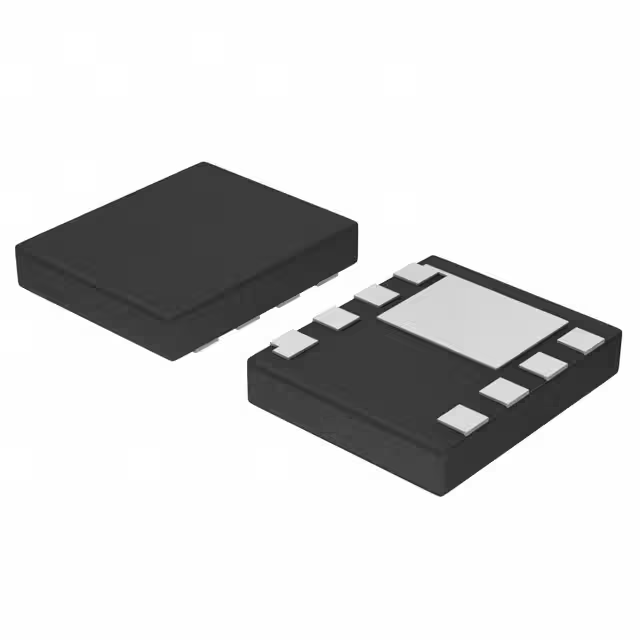
- Part No.:
- NUS3055MUTAG
- Manufacturer:
- onsemi
- Category:
- Mixed Technology
- Package:
- 8-UFLGA Exposed Pad
- Datasheet:
-
 NUS3055MUTAG.pdf
- Description:
- TVS DEVICE MIXED 7.08V 8-LLGA
- Quantity:
- Payment:

- Shipping:

Inventory:7,498
Please send an inquiry. Send us your inquiry, and we will respond immediately.
Product details
Overview
NUS3055MUTAG from onsemi is a low-profile overvoltage protection IC with an integrated −30 V P-channel MOSFET, designed to safeguard portable electronics against input overvoltage transients and supply faults. It features a nominal 6.85 V overvoltage threshold, 2.8 V undervoltage lockout, 75 mΩ RDS(on) at −4.5 V, and operates in a 2.5 × 3.0 mm TLLGA8 package - ideal for single-cell Li-ion and 3/4-cell NiMH/NiCd battery-powered devices such as smartphones and digital cameras.
For engineers reviewing the NUS3055MUTAG datasheet, pinout, applications, or equivalent options, key selection considerations include its fast <1.0 µs overvoltage turn-off time, integrated FET gate drive capability, accurate ±2.0% UVLO threshold, and compatibility with AC-DC adapters and car accessory chargers in space-constrained portable systems.
Technical Context
The NUS3055MUTAG integrates an overvoltage protection circuit (OVP) and a −30 V P-channel power MOSFET into a single die-level assembly. Its OVP core monitors the IN pin voltage and drives the OUT pin to disconnect the FET when VIN exceeds 6.85 V (±2.0% typical accuracy), with <1.0 µs response under ≤12 nF load capacitance.
It supports dual control modes: autonomous overvoltage cutoff and logic-controlled enable/disable via the CNTRL pin (VIH = 1.5 V, VIL = 0.5 V). Undervoltage lockout activates below 2.8 V (nominal) on VCC, ensuring safe FET disablement during brownout conditions - critical for battery-backed portable systems.
Key Specifications
| Parameter | Value and Actual Design Meaning |
|---|---|
| OVP Threshold | 6.85 V nominal, ±2.0% accuracy - enables precise protection for 4.2 V Li-ion systems without external resistive divider |
| UVLO Threshold | 2.8 V nominal, ±0.3 V range - prevents erratic operation during battery discharge below safe operating voltage |
| RDS(on) | 75 mΩ max at VGS = −4.5 V, ID = 600 mA - minimizes conduction loss and self-heating in 1 A portable power paths |
| Turn-off Delay | <1.0 µs (IN-triggered, CL ≤ 12 nF) - ensures sub-microsecond disconnection before transient energy damages downstream ICs |
| Package Height | 0.55 mm max - fits ultra-thin mobile designs where Z-height is constrained by mechanical stack-up |
| Supply Current | 0.75–1.0 mA at VCC = 6.0 V - enables always-on protection without significant battery drain in standby |
| ESD Rating | 2.5 kV HBM (pins 1,2,3,7,8) - meets IEC 61000-4-2 Level 2 for robust handling in manufacturing and end-user environments |
Pinout & Package
The NUS3055MUTAG is housed in a Pb-free, 2.5 × 3.0 mm, 0.55 mm profile TLLGA8 (Case 517AH) package with exposed thermal pad on bottom side for enhanced heat dissipation in high-current portable applications.
| Pin/Terminal | Circuit Role | Design Meaning |
|---|---|---|
| 1 IN | OVP sense input | Monitors input rail voltage; triggers FET shutdown if >6.85 V; supports threshold adjustment via external resistor to VCC |
| 2 GND | Power ground reference | Common return path for OVP logic, FET source, and internal regulator - must be low-impedance connection to PCB ground plane |
| 3 CNTRL | Logic enable/disable control | Active-high signal (VIH ≥ 1.5 V) forces FET off regardless of IN voltage - used for system-level power sequencing or fault recovery |
| 4 DRAIN | MOSFET drain terminal | Connects to input supply (e.g., adapter output); withstands −30 V VDSS - placed upstream of protected load |
| 5 SRC | MOSFET source terminal | Connects to load side; forms current path with DRAIN; tied to GND through load - defines forward conduction direction |
| 6 GATE | MOSFET gate terminal | Internally driven by OUT; not user-accessible - eliminates need for external gate driver or level shifter |
| 7 OUT | FET gate drive output | Drives GATE to within 1.0 V of VCC to turn off P-FET; sinks up to 50 µA - compatible with standard logic-level control |
| 8 VCC | IC supply input | Power source for OVP logic and driver; UVLO disables OUT if <2.5 V - ensures fail-safe behavior during low-battery conditions |
Key Features
| Feature | Design Value |
|---|---|
| Integrated −30 V P-channel MOSFET | Eliminates discrete FET + driver BOM, reduces PCB area by >40% vs. discrete OVP solutions |
| Sub-1 µs overvoltage response | Prevents latch-up or permanent damage in microprocessor ports and USB peripherals during 12 V adapter plug-in transients |
| Accurate 2.0% UVLO threshold | Enables reliable low-voltage cutoff before Li-ion cell reaches 2.8 V, preserving battery cycle life and safety margin |
| 0.55 mm profile TLLGA8 package | Supports <9.5 mm total device thickness in clamshell phones and ultraportable tablets with tight mechanical envelopes |
| Pb-free reflow compatibility | Rated for peak solder temperature up to 260°C - compliant with IPC/JEDEC J-STD-020D for lead-free assembly processes |
Applications
| Smartphone Power Input Protection | Digital Camera Battery Charging Circuit |
|---|---|
Use Scenario: AC adapter or car charger connected to smartphone mainboard during charging or data transfer. IC Role / Device Role / Timing Role: Overvoltage protector placed between input connector and PMIC/battery charger IC. Use Value: Disables input path in <1.0 µs if adapter outputs >6.85 V due to regulation failure - preventing damage to 3.3 V/1.8 V SoC rails. |
Use Scenario: External 5 V USB power applied to camera while internal Li-ion battery is charging. IC Role / Device Role / Timing Role: High-side switch isolating USB input from battery charging IC and sensor subsystem. Use Value: Blocks reverse current and overvoltage spikes from faulty chargers, leveraging 75 mΩ RDS(on) to minimize voltage drop during 1 A charging. |
| Portable Medical Monitor Power Path | Handheld Barcode Scanner Input Stage |
Use Scenario: Field-deployed patient monitor powered via universal AC-DC adapter in varying global voltage environments. IC Role / Device Role / Timing Role: Primary overvoltage guard before DC-DC converters and analog front-end circuits. Use Value: 6.85 V threshold aligns with 5 V ±10% adapter tolerance; 2.8 V UVLO prevents brownout-induced firmware crashes during battery switchover. |
Use Scenario: Industrial barcode scanner using automotive cigarette-lighter adapter in warehouse vehicles. IC Role / Device Role / Timing Role: Input protection stage upstream of 3.3 V MCU and laser driver IC. Use Value: Withstands 24 V load-dump transients via −30 V VDSS rating and shuts down in <1 µs - protecting sensitive CMOS logic from ESD-coupled surges. |
Equivalent & Alternatives
The following parts are listed as comparable options for similar overvoltage protection applications.
| Alternative Part | Technical Difference | Application Difference | Selection Advice |
|---|---|---|---|
| TPS259210DRCT | −20 V rated, 28 mΩ RDS(on), no integrated FET - requires external MOSFET | Designed for higher-current (5 A) USB PD applications; lacks built-in FET integration | Select when higher current capacity and programmable OVP threshold are required; adds layout complexity and BOM cost |
| NCP345MUTAG | Same OVP core but no integrated MOSFET - requires external P-FET and gate driver | Legacy solution for designs needing flexible FET selection (e.g., different VDSS/RDS(on)) | Choose only if discrete FET optimization is mandatory; NUS3055MUTAG offers superior integration and smaller footprint |
Compared with TPS259210DRCT and NCP345MUTAG, the NUS3055MUTAG delivers lowest component count and smallest PCB area for ≤1 A portable overvoltage protection, trading off adjustable threshold and higher current capability for guaranteed space and reliability advantages in thin-profile consumer devices.
Availability
NUS3055MUTAG is available at Aetrix Electronics and suitable for portable computers and PDAs, cell phones and handheld products, and digital cameras requiring stable component supply across high-volume production cycles and long-term design-in support.
Supply support for NUS3055MUTAG includes scheduled delivery planning, volume procurement assistance, BOM continuity management, traceable sourcing, and lifecycle availability coordination for OEM customers, industrial embedded developers, connected-device designers, and electronics production programs.
Manufacturer
onsemi (formerly ON Semiconductor) is a global semiconductor supplier focused on energy-efficient innovation for automotive, industrial, cloud, medical, and IoT applications - delivering silicon solutions that reduce power consumption and improve system reliability.
The NUS3055MUTAG belongs to onsemi's integrated protection IC product line, engineered specifically for compact, high-reliability overvoltage and undervoltage protection in battery-powered portable electronics - emphasizing minimal footprint, fast response, and seamless adapter interoperability.
FAQ
What is the overvoltage threshold accuracy of the NUS3055MUTAG?
The NUS3055MUTAG has a nominal overvoltage threshold of 6.85 V with ±2.0% accuracy over temperature and process variation. This specification is verified per onsemi's Electrical Characteristics table (page 4 of datasheet NUS3055/D), ensuring consistent trip points across production lots and ambient temperatures from −40°C to +85°C - critical for protecting 4.2 V Li-ion systems without calibration.
Can the NUS3055MUTAG be used with a 12 V input supply?
No - the NUS3055MUTAG is rated for a maximum VDSS of −30 V and VIN/VVCC of 30 V, but its 6.85 V overvoltage threshold makes it unsuitable for direct 12 V operation. Applying 12 V to IN would immediately trigger shutdown. It is intended for 5 V adapter inputs (e.g., USB, car chargers) where overvoltage events exceed 6.85 V, not for nominal 12 V systems. For 12 V applications, consider higher-threshold alternatives like NCP346.
Does the NUS3055MUTAG require an external gate resistor for the integrated MOSFET?
No - the NUS3055MUTAG integrates the gate driver and does not expose the GATE pin externally (pin 6 is internal-only). The OUT pin (pin 7) drives the gate directly, and the internal driver is optimized for ≤12 nF total gate + stray capacitance. No external gate resistor is needed or recommended; adding one would degrade the <1.0 µs turn-off performance specified in the datasheet.
How does the CNTRL pin interact with overvoltage detection in the NUS3055MUTAG?
The CNTRL pin (pin 3) provides priority override: when driven high (≥1.5 V), it forces the OUT pin high and turns off the MOSFET regardless of IN voltage - even if IN is below 6.85 V. When low (≤0.5 V), normal OVP operation resumes. This allows system-level control (e.g., MCU-initiated power-down) independent of input conditions, as confirmed in the Truth Table on page 3 of the NUS3055/D datasheet.
What is the thermal performance of the NUS3055MUTAG under 1 A continuous load?
At 1 A continuous drain current, the NUS3055MUTAG dissipates ~75 mW (I²R = 1² × 0.075 Ω). With a junction-to-air thermal resistance of 124°C/W for the FET portion (page 3, Maximum Ratings), this yields ~9.3°C temperature rise above ambient - well within the 150°C max junction limit. Performance assumes proper PCB copper pour on the exposed pad per Case 517AH footprint guidelines in the datasheet.
NUS3055MUTAG Specifications
- Product attributes
- Attribute value
- Manufacturer:
- onsemi
- Package/Case:
- 8-UFLGA Exposed Pad
- Series:
- -
- Packaging:
- Tape & Reel (TR)
- Product Status:
- Obsolete
- Voltage - Clamping:
- 7.08V
- Technology:
- Mixed Technology
- Number of Circuits:
- 1
- Applications:
- General Purpose
- Grade:
- -
- Qualification:
- -
- Mounting Type:
- Surface Mount
- Supplier Device Package:
- 8-LLGA (3x2.5)
NUS3055MUTAG FAQ
1.How can I place an order for NUS3055MUTAG through Aetrix?
Please submit a Request for Quotation (RFQ) for NUS3055MUTAG on Aetrix. Our sales agent will provide a competitive quotation and guide you through the order confirmation once you accept the terms.
2.Are the price and stock information for NUS3055MUTAG reliable?
The price and inventory of NUS3055MUTAG are updated periodically and may fluctuate due to market conditions. Stock and pricing data are typically refreshed every 24 hours. Quotation validity for NUS3055MUTAG is usually 5 days.
3.What payment methods are accepted for NUS3055MUTAG?
We accept Wire Transfer, PayPal, Credit Card, Western Union, MoneyGram, and Escrow for NUS3055MUTAG transactions.
Note: Certain payment methods may incur a processing fee.
4.How is shipping managed for NUS3055MUTAG?
NUS3055MUTAG orders can be shipped via leading logistics carriers, including DHL, UPS, FedEx, TNT, or Registered Mail.
Once your NUS3055MUTAG order is processed, you will receive an email with the shipment details and tracking number.
Note: Tracking information may take up to 24 hours to appear. Express delivery typically takes 3–5 business days.
5.How can I obtain technical support or documentation for NUS3055MUTAG?
For technical support, including NUS3055MUTAG datasheets, pinout diagrams, or application guidance, please contact our engineering support team. They can provide detailed documentation and assistance for your NUS3055MUTAG requirements.
6.How does Aetrix verify that NUS3055MUTAG is sourced from the original manufacturer or authorized distributors?
All NUS3055MUTAG products on Aetrix are procured from qualified distributors and authorized channels. Our dedicated quality assurance team conducts strict verification, including traceability checks and, if necessary, third-party testing. This ensures that NUS3055MUTAG meets industry standards.
7.What is the process for return or replacement of NUS3055MUTAG?
All NUS3055MUTAG units undergo pre-shipment inspection (PSI). If there is an issue with NUS3055MUTAG, returns or replacements are accepted under the following conditions:
1.Quantity discrepancies, incorrect items, or visible external defects (such as breakage or corrosion), acknowledged by Aetrix.
2.The issue is reported within 90 days of delivery.
3.The NUS3055MUTAG part is unused and in its original packaging.
Return procedure for NUS3055MUTAG:
1.Submit a request within 90 days.
2.Obtain a Return Material Authorization (RMA) from Aetrix.
NUS3055MUTAG Tags
-
ESD03A5V5R17V
Stackpole Electronics Inc
-
ESDU02A5V5R17V
Stackpole Electronics Inc
-
0603ESDA-MLP7
Eaton - Electronics Division
.jpg)
-
0603ESDA2-TR2
Eaton - Electronics Division
-
PS04LTVA1
Eaton - Electronics Division
.jpg)
-
0402ESDA-MLP1
Eaton - Electronics Division
.jpg)
-
0402ESDA-MLP7
Eaton - Electronics Division
-
TPD2S017DBVR
Texas Instruments
.jpg)
-
V2F105A150Y2EDP
KYOCERA AVX
-
82307050029
Würth Elektronik
-
NCP360SNT1G
onsemi
-
V2F118A400Y2EDP
KYOCERA AVX
Tech Hub

Counterfeit components can hide behind convincing markings and passing basic function tests. This engineering reference covers source traceability, external inspection, X-ray, XRF, electrical testing, …

A practical engineering and sourcing framework covering lifecycle verification, lifetime-buy calculations, replacement qualification, supplier checks and counterfeit-risk controls.

TTL and CMOS logic families differ in thresholds, loading, output drive, power and timing. This engineering guide compares 74HC and 74HCT, calculates noise margins and checks 3.3 V/5 V compatibility.

A practical engineering guide to 3.3V and 5V logic compatibility, input thresholds, resistor dividers, translator ICs, MOSFET level shifting, I2C pull-ups, timing limits and power-sequencing risks.

The 74HC595 uses push-pull logic outputs, while the TPIC6B595 uses 50 V open-drain DMOS sinks for higher-power loads. This guide compares timing, current limits, 3.3 V interfacing, load wiring, thermal…

The 74HC595 converts serial data into eight stable parallel outputs. This guide covers pin functions, shift and storage timing, OE and MR behavior, drive-current limits, cascading, voltage compatibilit…

A technical comparison of level-sensitive latches and edge-triggered flip-flops, covering timing windows, setup and hold limits, master–slave operation, time borrowing, race-through, HDL inference and…

A D latch stores one bit while Enable controls when data can pass. This reference covers gate-level operation, truth tables, transparency, setup and hold timing, LE versus OE, common ICs and practical …

An SR latch stores one bit through cross-coupled feedback. This engineering reference covers NOR and NAND implementations, truth tables, forbidden-state recovery, gated operation, switch debouncing, fa…

Latch circuits retain one bit through feedback. This technical reference covers SR and D latches, truth tables, transparency, timing limits, latch-versus-flip-flop behavior, applications and common log…


