
 My Inquiry
 My Account


NXP Semiconductors NX3L1G66GW,125
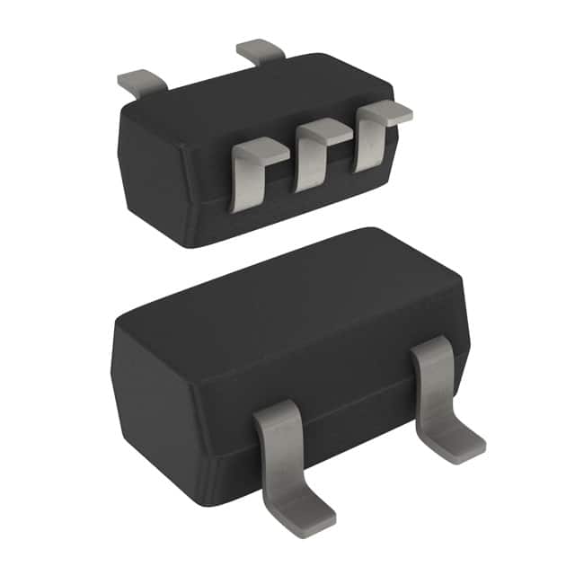
- Part No.:
- NX3L1G66GW,125
- Manufacturer:
- NXP Semiconductors
- Package:
- 5-TSSOP, SC-70-5, SOT-353
- Datasheet:
-
 NX3L1G66GW,125.pdf
- Description:
- IC SW SPST-NOX1 750MOHM 5TSSOP
- Quantity:
- Payment:

- Shipping:

Inventory:4,307
Please send an inquiry. Send us your inquiry, and we will respond immediately.
Product details
Overview
NX3L1G66GW,125 from NXP Semiconductors is a low-ohmic SPST analog switch in TSSOP5 package, featuring 0.5 Ω typical ON resistance at 2.7 V, Schmitt-trigger enable input (E), and bidirectional signal routing between Y and Z terminals. It operates from 1.4 V to 4.3 V supply and supports ±350 mA continuous switch current - ideal for audio path switching in portable consumer devices.
For engineers reviewing the NX3L1G66GW,125 datasheet, NX3L1G66GW,125 pinout, NX3L1G66GW,125 application, or NX3L1G66GW,125 equivalent, key selection criteria include ON-resistance flatness (0.13 Ω), −40 °C to +125 °C temperature range, ESD robustness (4 kV IEC61000-4-2 contact), and TTL-level compatibility at 3.0 V.
Technical Context
The NX3L1G66GW,125 implements a CMOS transmission gate architecture with Schmitt-trigger action on the active-HIGH enable pin (E), enabling reliable operation with slow-rising control signals. Its rail-to-rail analog signal handling (up to VCC) and low charge injection (3 pC at 1.5–3.3 V) support high-fidelity audio and precision sensor signal routing.
Static leakage is tightly controlled: OFF-state leakage ≤500 nA over −40 °C to +125 °C, and supply current remains below 7 µA at 4.3 V. Dynamic performance includes 14 ns enable time (VCC ≥ 2.7 V) and −90 dB OFF-state isolation at 100 kHz.
Key Specifications
| Parameter | Value and Actual Design Meaning |
|---|---|
| ON Resistance (typ) | 0.50 Ω at VCC = 2.7 V - ensures minimal voltage drop and signal attenuation in audio/headphone paths |
| ON Resistance Flatness (typ) | 0.13 Ω - maintains consistent gain and linearity across full analog signal swing (0 V to VCC) |
| Supply Voltage Range | 1.4 V to 4.3 V - supports single-supply operation in Li-ion (3.0–3.7 V) and dual-cell alkaline (2.4–3.2 V) systems |
| Operating Temperature | −40 °C to +125 °C - qualified for extended industrial and automotive-adjacent portable applications |
| ESD Robustness | 4 kV IEC61000-4-2 contact discharge on switch ports - reduces need for external protection in handheld interfaces |
| Switch Current Rating | ±350 mA continuous - sufficient for driving 16 Ω headphones or biasing MEMS microphones |
| Enable Propagation Delay | 14 ns (max) at VCC ≥ 2.7 V - enables fast channel reconfiguration in multi-source audio routing |
Pinout & Package
TSSOP5 (SOT353-1) package: plastic thin shrink small outline, 5-lead, body width 1.25 mm, pin 1 indicator at lower-left corner below marking code "DL".
| Pin/Terminal | Circuit Role | Design Meaning |
|---|---|---|
| 1 (Y) | Independent analog I/O terminal | Bidirectional signal path - connects to source (e.g., codec output) or load (e.g., speaker amplifier input) |
| 2 (Z) | Independent analog I/O terminal | Paired with Y; forms single-pole, single-throw switch path - no internal polarity or directionality |
| 3 (GND) | Ground reference | Return path for switch current and enable logic; must be low-impedance to minimize crosstalk and THD |
| 4 (E) | Active-HIGH enable input | Schmitt-triggered - tolerates slow edges; logic HIGH (>0.7VCC) closes switch, LOW opens it |
| 5 (VCC) | Positive supply rail | Defines analog signal range (0 V to VCC); powers internal logic and transmission gate - decoupling required |
Key Features
| Feature | Design Value |
|---|---|
| Rail-to-rail analog signal handling | Supports signals from 0 V to VCC - eliminates level-shifting needs in mixed-voltage portable systems |
| Low charge injection (3 pC) | Minimizes glitch-induced pop/click in audio switching - critical for headphone jack detection and mute control |
| High OFF-state isolation (−90 dB) | Prevents audible crosstalk between active and inactive audio channels in multi-input devices |
| TTL-compatible control at 3.0 V | Direct interface with 3.3 V GPIO without level shifters - simplifies host MCU integration |
| Wide VCC range (1.4–4.3 V) | Enables use across battery chemistries (Li-ion, NiMH, alkaline) without redesigning power domains |
Applications
| Smartphone Audio Routing | Portable Media Player |
|---|---|
Use Scenario: Switching between earpiece, loudspeaker, and headset outputs based on accessory detection. IC Role / Device Role / Timing Role: Bidirectional analog switch controlling audio path connectivity under GPIO control. Use Value: 0.5 Ω ON resistance and 0.13 Ω flatness preserve SNR and frequency response; −90 dB isolation prevents channel bleed. |
Use Scenario: Muting/unmuting left/right audio channels during track transitions or volume ramping. IC Role / Device Role / Timing Role: Low-latency (14 ns) SPST switch enabling glitch-free audio muting. Use Value: 3 pC charge injection eliminates audible pop; Schmitt-trigger E input rejects noise from shared PCB traces. |
| PDA Touchscreen Interface | Wearable Biometric Sensor Hub |
Use Scenario: Isolating touchscreen controller analog inputs during system sleep to reduce leakage current. IC Role / Device Role / Timing Role: Signal gate enabling/disabling analog front-end connection to ADC. Use Value: <500 nA OFF-state leakage at +125 °C extends battery life; 1.4 V minimum VCC supports ultra-low-power modes. |
Use Scenario: Multiplexing signals from optical heart-rate sensor, accelerometer, and temperature sensor to shared ADC. IC Role / Device Role / Timing Role: Low-distortion analog switch routing biometric sensor outputs without gain error. Use Value: 0.02% THD at 2.7 V ensures accurate pulse waveform capture; 60 MHz −3 dB bandwidth preserves signal integrity. |
Equivalent & Alternatives
The following parts are listed as comparable options for similar analog switch applications.
| Alternative Part | Technical Difference | Application Difference | Selection Advice |
|---|---|---|---|
| TS5A23157DCUR | Higher ON resistance (0.9 Ω typ at 3.3 V); no Schmitt trigger on enable; 0.5 mm pitch QFN-10 package | Limited to lower-frequency signal routing; requires clean enable edges; unsuitable for space-constrained TSSOP5 layouts | Select when board area allows QFN and control timing is tightly managed |
| ADG801BRM | Lower leakage (<100 pA OFF-state); higher ON resistance (0.8 Ω typ at 3 V); −40 °C to +85 °C only | Better for precision sensor multiplexing but not for high-current audio loads; narrower temp range excludes extended industrial use | Choose for ultra-low-leakage instrumentation where audio fidelity and wide temperature are secondary |
Compared with TS5A23157DCUR and ADG801BRM, the NX3L1G66GW,125 uniquely balances low ON resistance, Schmitt-trigger robustness, and extended temperature operation - making it optimal for cost-sensitive, space-constrained portable audio systems requiring reliable signal routing across battery voltage variation.
Availability
NX3L1G66GW,125 is available at Aetrix Electronics and suitable for smartphone audio routing, portable media player muting, and wearable biometric sensor hub applications requiring stable component supply across production lifecycles.
Supply support for NX3L1G66GW,125 includes scheduled delivery planning, volume procurement assistance, BOM continuity management, traceable sourcing, and lifecycle availability coordination for OEM customers, industrial embedded developers, connected-device designers, and electronics production programs.
Manufacturer
NXP Semiconductors is a global semiconductor company headquartered in Eindhoven, Netherlands, specializing in secure connectivity solutions for automotive, industrial, and consumer markets.
The NX3L series targets ultra-low-power, high-fidelity analog signal switching in battery-operated portable electronics - emphasizing rail-to-rail operation, minimal distortion, and robust ESD tolerance.
FAQ
What is the maximum continuous current rating for the NX3L1G66GW,125?
The NX3L1G66GW,125 supports ±350 mA continuous current at 3.3 V supply, verified per datasheet Table 5 (ISW). This rating applies under recommended operating conditions (Tamb ≤ +125 °C, VSW within 0 V to VCC). Exceeding this may cause thermal shutdown or parametric drift in ON resistance.
Does the NX3L1G66GW,125 support rail-to-rail analog signal transmission?
Yes, the NX3L1G66GW,125 allows signals with amplitude up to VCC to be transmitted bidirectionally between Y and Z terminals, as confirmed in Section 1 (General description) and Table 6 (VSW = 0 to VCC). This eliminates level-shifting requirements in single-supply portable systems.
What is the function of the Schmitt trigger on the enable pin (E) of the NX3L1G66GW,125?
The Schmitt trigger on the E pin provides hysteresis (VIH/VIL thresholds defined in Table 7), making the NX3L1G66GW,125 tolerant to slow-rising or noisy control signals - critical for GPIO-driven switching in electrically noisy handheld PCBs. It ensures clean, bounce-free turn-on/turn-off without external filtering.
Is the NX3L1G66GW,125 qualified for automotive applications?
No - the NX3L1G66GW,125 is specified for −40 °C to +125 °C operation but is not AEC-Q100 qualified. NXP explicitly states in Section 16.3 that non-automotive qualified products like NX3L1G66GW,125 are "not suitable for automotive use" and lack automotive-grade testing or warranty coverage.
How does the ON resistance flatness of the NX3L1G66GW,125 impact audio performance?
The NX3L1G66GW,125 exhibits 0.13 Ω typical ON resistance flatness (Table 8), meaning its resistance varies by ≤0.13 Ω across the full 0 V to VCC signal range. This minimizes harmonic distortion (0.02% THD at 2.7 V) and preserves frequency response - essential for high-fidelity headphone and speaker outputs.
NX3L1G66GW,125 Specifications
- Product attributes
- Attribute value
- Manufacturer:
- NXP Semiconductors
- Series:
- -
- Packaging:
- Tape & Reel (TR)
- Product Status:
- Obsolete
- Switch Circuit:
- SPST - NO
- Multiplexer/Demultiplexer Circuit:
- 1:1
- Number of Circuits:
- 1
- On-State Resistance (Max):
- 750mOhm
- Channel-to-Channel Matching (ΔRon):
- -
- Voltage - Supply, Single (V+):
- 1.4V ~ 4.3V
- Voltage - Supply, Dual (V±):
- -
- Switch Time (Ton, Toff) (Max):
- 23ns, 8ns
- -3db Bandwidth:
- 60MHz
- Charge Injection:
- 6pC
- Channel Capacitance (CS(off), CD(off)):
- 35pF
- Current - Leakage (IS(off)) (Max):
- 10nA
- Crosstalk:
- -
- Operating Temperature:
- -40°C ~ 125°C (TA)
- Grade:
- -
- Qualification:
- -
- Mounting Type:
- Surface Mount
- Supplier Device Package:
- 5-TSSOP
NX3L1G66GW,125 FAQ
1.How can I place an order for NX3L1G66GW,125 through Aetrix?
Please submit a Request for Quotation (RFQ) for NX3L1G66GW,125 on Aetrix. Our sales agent will provide a competitive quotation and guide you through the order confirmation once you accept the terms.
2.Are the price and stock information for NX3L1G66GW,125 reliable?
The price and inventory of NX3L1G66GW,125 are updated periodically and may fluctuate due to market conditions. Stock and pricing data are typically refreshed every 24 hours. Quotation validity for NX3L1G66GW,125 is usually 5 days.
3.What payment methods are accepted for NX3L1G66GW,125?
We accept Wire Transfer, PayPal, Credit Card, Western Union, MoneyGram, and Escrow for NX3L1G66GW,125 transactions.
Note: Certain payment methods may incur a processing fee.
4.How is shipping managed for NX3L1G66GW,125?
NX3L1G66GW,125 orders can be shipped via leading logistics carriers, including DHL, UPS, FedEx, TNT, or Registered Mail.
Once your NX3L1G66GW,125 order is processed, you will receive an email with the shipment details and tracking number.
Note: Tracking information may take up to 24 hours to appear. Express delivery typically takes 3–5 business days.
5.How can I obtain technical support or documentation for NX3L1G66GW,125?
For technical support, including NX3L1G66GW,125 datasheets, pinout diagrams, or application guidance, please contact our engineering support team. They can provide detailed documentation and assistance for your NX3L1G66GW,125 requirements.
6.How does Aetrix verify that NX3L1G66GW,125 is sourced from the original manufacturer or authorized distributors?
All NX3L1G66GW,125 products on Aetrix are procured from qualified distributors and authorized channels. Our dedicated quality assurance team conducts strict verification, including traceability checks and, if necessary, third-party testing. This ensures that NX3L1G66GW,125 meets industry standards.
7.What is the process for return or replacement of NX3L1G66GW,125?
All NX3L1G66GW,125 units undergo pre-shipment inspection (PSI). If there is an issue with NX3L1G66GW,125, returns or replacements are accepted under the following conditions:
1.Quantity discrepancies, incorrect items, or visible external defects (such as breakage or corrosion), acknowledged by Aetrix.
2.The issue is reported within 90 days of delivery.
3.The NX3L1G66GW,125 part is unused and in its original packaging.
Return procedure for NX3L1G66GW,125:
1.Submit a request within 90 days.
2.Obtain a Return Material Authorization (RMA) from Aetrix.
NX3L1G66GW,125 Tags

-
SN74LVC1G3157DBVR
Texas Instruments

-
SN74LVC1G66DBVR
Texas Instruments

-
SN74LVC1G66DCKR
Texas Instruments
-
SN74LVC1G3157DSFR
Texas Instruments

-
1P1G3157QDCKRQ1
Texas Instruments

-
SN74LVC2G66DCUR
Texas Instruments

-
SN74LV4052APWR
Texas Instruments
-
74HC4051D,653
Nexperia USA Inc.
-
SN74LV4051APWR
Texas Instruments
-
CD74HC4052PWR
Texas Instruments
-
CD74HC4051PWR
Texas Instruments
-
TS5A3166DBVR
Texas Instruments
Tech Hub

A practical engineering guide to 3.3V and 5V logic compatibility, input thresholds, resistor dividers, translator ICs, MOSFET level shifting, I2C pull-ups, timing limits and power-sequencing risks.

The 74HC595 uses push-pull logic outputs, while the TPIC6B595 uses 50 V open-drain DMOS sinks for higher-power loads. This guide compares timing, current limits, 3.3 V interfacing, load wiring, thermal…

The 74HC595 converts serial data into eight stable parallel outputs. This guide covers pin functions, shift and storage timing, OE and MR behavior, drive-current limits, cascading, voltage compatibilit…

A technical comparison of level-sensitive latches and edge-triggered flip-flops, covering timing windows, setup and hold limits, master–slave operation, time borrowing, race-through, HDL inference and…

A D latch stores one bit while Enable controls when data can pass. This reference covers gate-level operation, truth tables, transparency, setup and hold timing, LE versus OE, common ICs and practical …

An SR latch stores one bit through cross-coupled feedback. This engineering reference covers NOR and NAND implementations, truth tables, forbidden-state recovery, gated operation, switch debouncing, fa…

Latch circuits retain one bit through feedback. This technical reference covers SR and D latches, truth tables, transparency, timing limits, latch-versus-flip-flop behavior, applications and common log…

An engineering guide to LED driver operation, constant-current and constant-voltage outputs, linear and switching topologies, dimming, IC selection, calculations, replacement compatibility, and fault c…

Operational amplifier guide covering op amp basics, feedback, ideal vs real op amps, common configurations, buffer circuits, offset, bias current, gain-bandwidth, slew rate, rail-to-rail limits and sel…

Jumper cables guide covering safe connection order, red and black clamp placement, final ground connection, cable gauge, length, clamp quality, copper vs CCA cables, jump starter comparison and battery…


