
 My Inquiry
 My Account


Texas Instruments OMAP3503DCUS
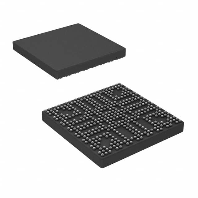
- Part No.:
- OMAP3503DCUS
- Manufacturer:
- Texas Instruments
- Category:
- Microprocessors
- Package:
- 423-LFBGA, FCBGA
- Datasheet:
-
 OMAP3503DCUS.pdf
- Description:
- IC MPU OMAP-35XX 600MHZ 423FCBGA
- Quantity:
- Payment:

- Shipping:

Inventory:2,102
Please send an inquiry. Send us your inquiry, and we will respond immediately.
Product details
Overview
OMAP3503DCUS from Texas Instruments is a 423-pin s-PBGA applications processor based on the ARM Cortex-A8 core, operating up to 720 MHz with 256-KB L2 cache, 112-KB ROM, and 64-KB shared SRAM. It integrates camera ISP, display subsystem with dual LCD support, SD/SDIO/MMC interfaces, and USB OTG/host - designed for portable media players and digital video cameras requiring high-resolution imaging and low-power operation.
For engineers reviewing the OMAP3503DCUS datasheet, OMAP3503DCUS pinout, OMAP3503DCUS application, or OMAP3503DCUS equivalent, key selection considerations include its CUS-package limitations (no POP interface, no discrete memory interface, reduced GPMC chip-selects), absence of PowerVR SGX graphics (vs. OMAP3515), and confirmed support for Linux, Android, and Windows CE in commercial/extended temperature grades.
Technical Context
The OMAP3503DCUS implements an ARMv7-compliant Cortex-A8 superscalar microprocessor with Thumb-2, NEON SIMD, TrustZone security, and dynamic branch prediction. Its memory subsystem includes SDRAM controller (SDRC) supporting LPDDR, General Purpose Memory Controller (GPMC) with eight chip-selects (though gpmc_ncs1/ncs2 and wait1/wait2 are omitted in CUS package), and SmartReflex AVS for adaptive voltage scaling between 0.985 V–1.35 V core logic.
It integrates dedicated hardware accelerators: Camera ISP with BT.601/BT.656 interface, resize engine (1/4× to 4×), color space converter, and dual 10-bit DACs for composite NTSC/PAL output. The display subsystem supports parallel RGB up to HD resolution, RFBI panels, and remote frame buffer interface - all without PowerVR SGX graphics (a key differentiator from OMAP3515).
Key Specifications
| Parameter | Value and Actual Design Meaning |
|---|---|
| Core Architecture | ARM Cortex-A8, in-order dual-issue superscalar, ARMv7 instruction set, Thumb-2 support |
| Max Operating Frequency | 720 MHz - enables real-time HD video decode and UI rendering in portable media devices |
| L2 Cache | 256 KB - reduces external memory bandwidth demand for multimedia workloads |
| On-chip Memory | 112 KB ROM + 64 KB shared SRAM - provides boot code storage and low-latency scratchpad for critical firmware |
| Process Technology | 65-nm CMOS - balances performance, power efficiency, and thermal density for handheld form factors |
| I/O Voltage | 1.8-V I/O, 0.985–1.35-V adaptive core logic - enables dynamic voltage scaling via SmartReflex for battery life extension |
| Package | 423-pin s-PBGA (CUS suffix), 0.65-mm ball pitch - compact footprint optimized for space-constrained portable designs |
Pinout & Package
The OMAP3503DCUS is housed in a 423-ball s-PBGA package (CUS suffix) with 0.65-mm ball pitch, no POP interface, and no discrete memory interface. Ball assignments follow TI's SPRS505H datasheet Section 2.2.1 (Figure 2-5 and Quadrant D maps), with key functional groups including SDRC, GPMC, DSS, ISP, MMC/SDIO, USB, UART, McSPI, McBSP, I²C, timers, and GPIO.
| Pin/Terminal | Circuit Role | Design Meaning |
|---|---|---|
| sdrc_d0–sdrc_d31 | SDRAM Data Bus | 32-bit bidirectional data path for LPDDR/SDRAM interfacing; requires matched trace lengths and termination |
| sdrc_a0–sdrc_a14 | SDRAM Address Bus | 15-bit address bus for up to 1 GB address space; multiplexed with bank address (ba0/ba1) |
| gpmc_ncs0–gpmc_ncs7 | GPMC Chip Select | Eight chip-select outputs; ncs1/ncs2 not available in CUS package per Table 1-1 |
| dss_data0–dss_data23 | Display Data Bus | 24-bit parallel RGB interface supporting HD resolution; configurable for YUV or RGB pixel formats |
| cam_d0–cam_d11 | Camera Parallel Interface | 12-bit parallel input for CCD/CMOS sensors; supports BT.601 (8-bit) and BT.656 (10-bit) YCbCr 4:2:2 |
| mmc1_clk / mmc1_cmd / mmc1_dat0–7 | MMC/SDIO Interface | Full 4-bit SD/SDIO v2.0 support with embedded card-detect and write-protect sensing |
Key Features
| Feature | Design Value |
|---|---|
| ARM Cortex-A8 Core | 720-MHz superscalar execution with NEON SIMD coprocessor - delivers >2× ARMv6 integer/FPU throughput for video codecs |
| Camera ISP | Hardware-accelerated image pipeline with resize (1/4× to 4×), color space conversion, and BT.601/BT.656 capture - offloads CPU during video recording |
| Dual Display Support | Simultaneous RGB LCD + TV-out (NTSC/PAL) via dual 10-bit DACs - enables split-screen UI and media playback on separate displays |
| SmartReflex AVS | Real-time adaptive voltage scaling across OPP points - reduces active power by up to 30% vs. fixed-voltage operation |
| USB 2.0 OTG + Host | Integrated ULPI PHY with 12-/8-pin interface - eliminates external transceiver for peripheral connectivity and device-host switching |
Applications
| Portable Media Player | Digital Video Camera |
|---|---|
Use Scenario: High-resolution video playback with touch UI and wireless streaming in handheld consumer devices. IC Role / Device Role / Timing Role: Main applications processor executing Android/Linux OS, decoding H.264/VC-1 streams, driving RGB LCD, and managing SD card storage. Use Value: Integrated ISP and display subsystem eliminate external video co-processors; 720-MHz Cortex-A8 ensures smooth 720p playback at ≤350 mW typical power. | Use Scenario: Real-time HD video capture, preview, and encoding in compact camcorders with optical zoom and stereo audio. IC Role / Device Role / Timing Role: Central imaging processor handling sensor interface, hardware-based image resizing, color correction, and HDMI/TV-out generation. Use Value: BT.656-compatible 10-bit ISP input and dual DACs enable direct analog video output without external encoder; SmartReflex extends battery runtime during continuous recording. |
| Web Tablet | Point-of-Sale Terminal |
Use Scenario: Cost-sensitive, fanless tablet for web browsing, document viewing, and light productivity in education or retail environments. IC Role / Device Role / Timing Role: Primary SoC running Android, managing resistive/capacitive touchscreen, Wi-Fi/BT connectivity, and dual-display UI rendering. Use Value: CUS package's 423-pin count and absence of POP reduce BOM cost and PCB layer count; integrated USB OTG supports peripheral docking without hub ICs. | Use Scenario: Ruggedized handheld terminal for inventory management, barcode scanning, and receipt printing in warehouse or field logistics. IC Role / Device Role / Timing Role: Embedded controller interfacing with 1D/2D barcode scanner, thermal printer, and secure payment module via UART/McSPI/GPIO. Use Value: 188 GPIO pins (muxed) and five UARTs allow concurrent peripheral control; extended temperature grade (-40°C to +105°C) ensures reliability in industrial ambient conditions. |
Equivalent & Alternatives
The following parts are listed as comparable options for similar applications processor applications.
| Alternative Part | Technical Difference | Application Difference | Selection Advice |
|---|---|---|---|
| OMAP3515CBB | Includes PowerVR SGX 3D graphics accelerator; 515-pin s-PBGA with POP support; higher pin count and thermal envelope | Required for OpenGL ES 2.0 gaming or complex UI rendering; unsuitable where CUS footprint or cost constraints apply | Select OMAP3515CBB only when 3D graphics acceleration is mandatory and board area allows larger package |
| i.MX535CJM | Freescale i.MX53 Cortex-A8 @ 1 GHz; integrated Vivante GC880 GPU; different memory controller (DDR2/DDR3), peripheral set, and boot architecture | Better suited for automotive infotainment or medical displays needing higher clock stability and DDR3 support | Choose i.MX535CJM for new designs requiring DDR3, longer vendor support, or ASIL-B readiness - not drop-in compatible |
Compared with OMAP3515CBB, OMAP3503DCUS omits PowerVR SGX and POP capability to reduce cost and size, making it optimal for imaging-centric but graphics-light applications; versus i.MX535CJM, it offers tighter integration with TI's DaVinci software stack and legacy Linux BSPs but lacks DDR3 and newer security features.
Availability
OMAP3503DCUS is available at Aetrix Electronics and suitable for portable media players, digital video cameras, and point-of-sale terminals requiring stable component supply, long-lifecycle support, and qualified industrial-grade silicon.
Supply support for OMAP3503DCUS includes scheduled delivery planning, volume procurement assistance, BOM continuity management, traceable sourcing, and lifecycle availability coordination for OEM customers, industrial embedded developers, connected-device designers, and electronics production programs.
Manufacturer
Texas Instruments is a global semiconductor leader specializing in analog, embedded processing, and connectivity technologies with over 90 years of innovation in industrial, automotive, and consumer electronics.
The OMAP3503 belongs to TI's OMAP™3 family of applications processors, engineered specifically for portable multimedia devices demanding high-performance video processing, low-power operation, and rich peripheral integration - without requiring 3D graphics acceleration.
FAQ
What is the maximum supported SDRAM capacity for OMAP3503DCUS?
The OMAP3503DCUS supports up to 1 GB of total external memory address space via its SDRAM Controller (SDRC), configured across LPDDR or mobile SDRAM devices. This capacity is achieved using 15-bit row/column addressing and two bank address bits (BA0/BA1), enabling configurations such as 128M×8 or 64M×16 devices. The CUS package retains full SDRC functionality despite omitting POP and discrete memory interfaces.
Does OMAP3503DCUS include PowerVR SGX graphics hardware?
No, OMAP3503DCUS does not include PowerVR SGX graphics acceleration. That feature is exclusive to the OMAP3515 variant. The OMAP3503DCUS shares the same ARM Cortex-A8 core, ISP, display subsystem, and peripheral set but omits the SGX engine - confirmed in Section 1.3 of SPRS505H and functional block diagram (Figure 1-1). Graphics rendering relies solely on CPU-based libraries or optional third-party IP.
Which operating systems are officially supported on OMAP3503DCUS?
OMAP3503DCUS officially supports Linux®, Windows® CE, and Android™, as documented in Section 1.3 of the SPRS505H datasheet. TI provided validated BSPs and kernel patches for these OSes during the product's active lifecycle. No official support exists for QNX, FreeRTOS, or bare-metal RTOSes beyond community ports.
What are the key package-level differences between OMAP3503DCUS and OMAP3515CBB?
OMAP3503DCUS uses a 423-pin s-PBGA (CUS) package with 0.65-mm pitch and no POP interface, while OMAP3515CBB uses a 515-pin s-PBGA (CBB) with 0.5-mm top/0.4-mm bottom pitch and full POP support. Per Table 1-1, CUS omits gpmc_ncs1/ncs2, gpmc_wait1/wait2, HSUSB3_TLL, MM_FSUSB3, and McSPI1 CS1/CS2 - reducing pin count and cost for non-POP designs.
Can OMAP3503DCUS drive dual independent displays simultaneously?
Yes, OMAP3503DCUS supports dual independent displays: one via its parallel RGB interface (up to 24-bit HD resolution) and a second via composite NTSC/PAL output using its two integrated 10-bit DACs. The display subsystem includes three overlay layers and temporal dithering, enabling simultaneous UI rendering on LCD and video playback on TV - confirmed in Section 1.1 and Figure 1-1 of SPRS505H.
OMAP3503DCUS Specifications
- Product attributes
- Attribute value
- Manufacturer:
- Texas Instruments
- Package/Case:
- 423-LFBGA, FCBGA
- Series:
- OMAP-35xx
- Packaging:
- Tray
- Product Status:
- Obsolete
- Core Processor:
- ARM® Cortex®-A8
- Number of Cores/Bus Width:
- 1 Core, 32-Bit
- Speed:
- 600MHz
- Co-Processors/DSP:
- Multimedia; NEON™ SIMD
- RAM Controllers:
- LPDDR
- Graphics Acceleration:
- No
- Display & Interface Controllers:
- LCD
- Ethernet:
- -
- SATA:
- -
- USB:
- USB 1.x (3), USB 2.0 (1)
- Voltage - I/O:
- 1.8V, 3.0V
- Operating Temperature:
- 0°C ~ 90°C (TJ)
- Grade:
- -
- Qualification:
- -
- Security Features:
- -
- Mounting Type:
- Surface Mount
- Supplier Device Package:
- 423-FCBGA (16x16)
- Additional Interfaces:
- HDQ/1-Wire, I2C, McBSP, McSPI, MMC/SD/SDIO, UART
OMAP3503DCUS FAQ
1.How can I place an order for OMAP3503DCUS through Aetrix?
Please submit a Request for Quotation (RFQ) for OMAP3503DCUS on Aetrix. Our sales agent will provide a competitive quotation and guide you through the order confirmation once you accept the terms.
2.Are the price and stock information for OMAP3503DCUS reliable?
The price and inventory of OMAP3503DCUS are updated periodically and may fluctuate due to market conditions. Stock and pricing data are typically refreshed every 24 hours. Quotation validity for OMAP3503DCUS is usually 5 days.
3.What payment methods are accepted for OMAP3503DCUS?
We accept Wire Transfer, PayPal, Credit Card, Western Union, MoneyGram, and Escrow for OMAP3503DCUS transactions.
Note: Certain payment methods may incur a processing fee.
4.How is shipping managed for OMAP3503DCUS?
OMAP3503DCUS orders can be shipped via leading logistics carriers, including DHL, UPS, FedEx, TNT, or Registered Mail.
Once your OMAP3503DCUS order is processed, you will receive an email with the shipment details and tracking number.
Note: Tracking information may take up to 24 hours to appear. Express delivery typically takes 3–5 business days.
5.How can I obtain technical support or documentation for OMAP3503DCUS?
For technical support, including OMAP3503DCUS datasheets, pinout diagrams, or application guidance, please contact our engineering support team. They can provide detailed documentation and assistance for your OMAP3503DCUS requirements.
6.How does Aetrix verify that OMAP3503DCUS is sourced from the original manufacturer or authorized distributors?
All OMAP3503DCUS products on Aetrix are procured from qualified distributors and authorized channels. Our dedicated quality assurance team conducts strict verification, including traceability checks and, if necessary, third-party testing. This ensures that OMAP3503DCUS meets industry standards.
7.What is the process for return or replacement of OMAP3503DCUS?
All OMAP3503DCUS units undergo pre-shipment inspection (PSI). If there is an issue with OMAP3503DCUS, returns or replacements are accepted under the following conditions:
1.Quantity discrepancies, incorrect items, or visible external defects (such as breakage or corrosion), acknowledged by Aetrix.
2.The issue is reported within 90 days of delivery.
3.The OMAP3503DCUS part is unused and in its original packaging.
Return procedure for OMAP3503DCUS:
1.Submit a request within 90 days.
2.Obtain a Return Material Authorization (RMA) from Aetrix.
OMAP3503DCUS Tags

-
AT91SAM9260B-CU-999
Microchip Technology
-
AT91SAM9G25-CU
Microchip Technology

-
ATSAMA5D27C-CU
Microchip Technology
-
AT91SAM9X35-CU
Microchip Technology
-
AT91SAM9X25-CU
Microchip Technology

-
MCIMX6Y2CVM08AB
NXP Semiconductors
.JPG)
-
AM3352BZCZ100
Texas Instruments
-
AT91SAM9260B-CU
Microchip Technology

-
AT91SAM9260B-QU
Microchip Technology

-
ATSAMA5D31A-CU
Microchip Technology
-
AT91SAM9G20B-CU-999
Microchip Technology
-
MCIMX6Y2CVM05AB
NXP Semiconductors
Tech Hub

A practical engineering guide to 3.3V and 5V logic compatibility, input thresholds, resistor dividers, translator ICs, MOSFET level shifting, I2C pull-ups, timing limits and power-sequencing risks.

The 74HC595 uses push-pull logic outputs, while the TPIC6B595 uses 50 V open-drain DMOS sinks for higher-power loads. This guide compares timing, current limits, 3.3 V interfacing, load wiring, thermal…

The 74HC595 converts serial data into eight stable parallel outputs. This guide covers pin functions, shift and storage timing, OE and MR behavior, drive-current limits, cascading, voltage compatibilit…

A technical comparison of level-sensitive latches and edge-triggered flip-flops, covering timing windows, setup and hold limits, master–slave operation, time borrowing, race-through, HDL inference and…

A D latch stores one bit while Enable controls when data can pass. This reference covers gate-level operation, truth tables, transparency, setup and hold timing, LE versus OE, common ICs and practical …

An SR latch stores one bit through cross-coupled feedback. This engineering reference covers NOR and NAND implementations, truth tables, forbidden-state recovery, gated operation, switch debouncing, fa…

Latch circuits retain one bit through feedback. This technical reference covers SR and D latches, truth tables, transparency, timing limits, latch-versus-flip-flop behavior, applications and common log…

An engineering guide to LED driver operation, constant-current and constant-voltage outputs, linear and switching topologies, dimming, IC selection, calculations, replacement compatibility, and fault c…

Operational amplifier guide covering op amp basics, feedback, ideal vs real op amps, common configurations, buffer circuits, offset, bias current, gain-bandwidth, slew rate, rail-to-rail limits and sel…

Jumper cables guide covering safe connection order, red and black clamp placement, final ground connection, cable gauge, length, clamp quality, copper vs CCA cables, jump starter comparison and battery…


