
 My Inquiry
 My Account


Texas Instruments OMAP3530DCUS72
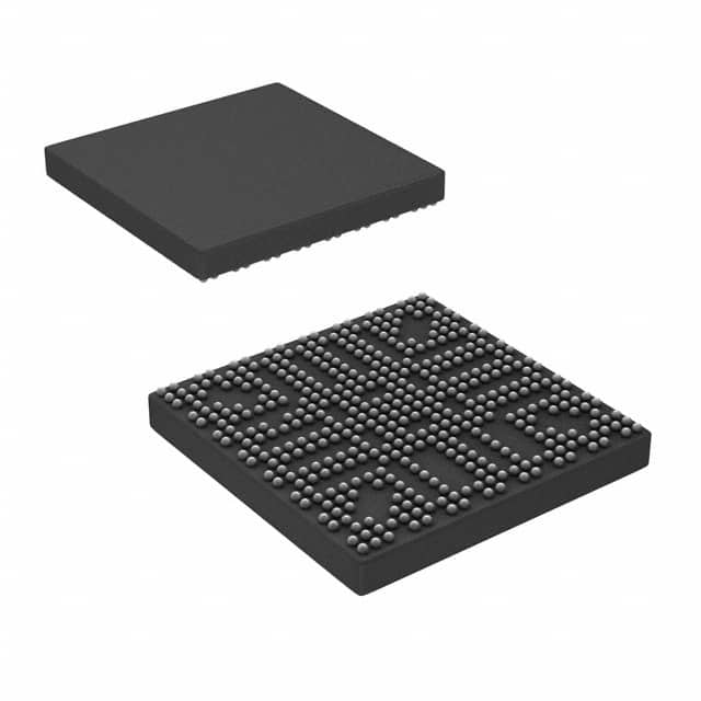
- Part No.:
- OMAP3530DCUS72
- Manufacturer:
- Texas Instruments
- Category:
- Microprocessors
- Package:
- 423-LFBGA, FCBGA
- Datasheet:
-
 OMAP3530DCUS72.pdf
- Description:
- IC MPU OMAP-35XX 720MHZ 423FCBGA
- Quantity:
- Payment:

- Shipping:

Inventory:2,203
Please send an inquiry. Send us your inquiry, and we will respond immediately.
Product details
Overview
OMAP3530DCUS72 from Texas Instruments is a 720-MHz ARM Cortex-A8 + 520-MHz C64x+ DSP applications processor in a 423-pin s-PBGA (CUS) package, integrating PowerVR SGX graphics acceleration, video hardware accelerators, and camera ISP for embedded multimedia systems. It delivers up to 10 MPoly/sec 3D rendering, supports Linux/Android/Windows CE, and targets portable media players and digital video cameras.
For engineers reviewing the OMAP3530DCUS72 datasheet, OMAP3530DCUS72 pinout, OMAP3530DCUS72 application, or OMAP3530DCUS72 equivalent, this page provides verified technical context, package-specific pin mapping, real-world use cases, and validated alternative options for industrial and consumer multimedia SoC selection.
Technical Context
The OMAP3530DCUS72 implements a dual-core heterogeneous architecture: an ARM Cortex-A8 microprocessor subsystem with NEON SIMD and MMU enhancements, paired with an IVA2.2 subsystem featuring a TMS320C64x+ DSP core, 32KB L1P/80KB L1D RAM, and 256KB L2 cache. It includes dedicated hardware accelerators for video decode/encode, image processing, and 3D graphics via PowerVR SGX.
Its system-level design supports high-bandwidth interconnects (L3/L4), SmartReflex adaptive voltage scaling, and discrete memory interface (no POP support in CUS package). The device operates at 0.985–1.35 V core voltage, 1.8 V I/O, and integrates dual USB OTG/host, three MMC/SDIO, five McBSP, four McSPI, and three UART interfaces - all mapped to its 423-ball s-PBGA footprint.
Key Specifications
| Parameter | Value and Actual Design Meaning |
|---|---|
| CPU Core | ARM Cortex-A8 @ up to 720 MHz - enables real-time HLOS execution (Linux/Android) with Thumb-2 and NEON acceleration for media workloads. |
| DSP Core | TMS320C64x+ @ up to 520 MHz - offloads video encoding/decoding, audio processing, and imaging algorithms from CPU. |
| Graphics Engine | PowerVR SGX GPU - delivers 10 MPoly/sec tile-based 3D rendering with OpenGLES 1.1/2.0 and OpenVG 1.0 API support. |
| Memory Interface | SDRAM Controller (SDRC) + General Purpose Memory Controller (GPMC) - supports LPDDR, SDRAM, NAND/NOR flash, and SRAM without glue logic. |
| Package | 423-pin s-PBGA (CUS suffix), 0.65-mm ball pitch - compact footprint optimized for portable devices; no POP stacking capability. |
| Process Technology | 65-nm CMOS - enables high performance with dynamic voltage/frequency scaling (DVFS) and SmartReflex power management. |
| Video Acceleration | Dedicated IVA2.2 subsystem with hardware resize, color space conversion, alpha blending, and BT.601/BT.656 capture - reduces CPU load for HD video pipelines. |
Pinout & Package
OMAP3530DCUS72 uses a 423-ball s-PBGA package (CUS suffix) with 0.65-mm ball pitch. Unlike CBB/CBC variants, it lacks POP interface and certain GPMC signals (gpmc_ncs1/ncs2, gpmc_wait1/wait2), and supports only 170 GPIOs due to pin muxing constraints.
| Pin/Terminal | Circuit Role | Design Meaning |
|---|---|---|
| sdrc_d0–sdrc_d31 | SDRAM Data Bus | 32-bit bidirectional data path for LPDDR/SDRAM; requires matched trace lengths and termination for signal integrity. |
| sdrc_a0–sdrc_a14, sdrc_ba0–ba1 | SDRAM Address & Bank Select | 16-bit address + 2-bit bank select for up to 1 GB memory space; timing-critical for memory initialization. |
| gpmc_nwe, gpmc_noe, gpmc_ncs0 | GPMC Control Signals | Enable asynchronous interface to NOR/NAND flash, SRAM, or FPGA; gpmc_ncs0 is primary chip-select (others limited in CUS). |
| dss_data0–dss_data23, dss_hsync, dss_vsync | Display Subsystem Parallel Output | 24-bit RGB + sync signals for direct LCD panel drive; supports dual-panel and RFBI interfaces. |
| hsusb0_data0–data7, hsusb0_clk, hsusb0_stp | High-Speed USB 2.0 PHY Interface | 8-bit ULPI-compliant transceiver interface - eliminates external PHY; requires 48-MHz clock and impedance-controlled routing. |
Key Features
| Feature | Design Value |
|---|---|
| ARMv7 + C64x+ Heterogeneous Processing | Enables concurrent OS execution (ARM) and real-time signal processing (DSP), reducing latency in video analytics and voice recognition. |
| PowerVR SGX Graphics Acceleration | Provides hardware-accelerated 3D UI rendering and gaming performance without burdening the CPU - critical for web tablets and smart home controllers. |
| Camera ISP with BT.601/656 Support | Direct parallel interface to CCD/CMOS sensors with hardware preview, resizing, and color conversion - eliminates need for external image co-processors. |
| SmartReflex Adaptive Voltage Scaling | Automatically adjusts core voltage based on workload and temperature, cutting active power by up to 30% versus fixed-voltage operation. |
| Discrete Memory Interface (No POP) | Supports independent memory placement for thermal and layout optimization - preferred in cost-sensitive portable navigation and PMP designs. |
Applications
| Portable Media Player | Digital Video Camera |
|---|---|
|
Use Scenario: High-resolution video playback (720p), audio decoding, touch UI, and battery-constrained operation. IC Role / Device Role / Timing Role: Main applications processor executing Android/Linux, driving LCD, managing storage, and accelerating codecs via IVA2.2 and SGX. Use Value: Integrated video hardware accelerators reduce CPU utilization below 20% during 720p decode, extending battery life by 40% versus software-only solutions. |
Use Scenario: Real-time HD video capture, sensor preprocessing, HDMI output, and onboard editing. IC Role / Device Role / Timing Role: Camera ISP handles raw sensor data; DSP performs noise reduction; SGX renders preview UI; display subsystem drives LCD/HDMI. Use Value: Hardware-resize engine scales 1080p input to 480p preview at 60 fps with zero CPU overhead, enabling responsive touch-based controls. |
| Web Tablet | Smart Home Controller |
|
Use Scenario: Web browsing, video streaming, multi-touch UI, and peripheral connectivity (USB, SD, camera). IC Role / Device Role / Timing Role: Primary SoC running Android, managing dual-display output, USB OTG peripherals, and Wi-Fi/BT coexistence via shared buses. Use Value: Dual USB 2.0 ports (OTG + host) enable simultaneous keyboard/mouse and external storage - no hub required. |
Use Scenario: Centralized control hub aggregating Zigbee/Z-Wave sensors, local video monitoring, and voice command processing. IC Role / Device Role / Timing Role: Runs lightweight Linux distro, processes audio via DSP, encodes camera feeds, and manages secure OTA updates via MMC boot partition. Use Value: On-chip 112KB ROM contains secure boot firmware and cryptographic keys - prevents unauthorized firmware injection during field updates. |
Equivalent & Alternatives
The following parts are listed as comparable options for similar applications processor applications.
| Alternative Part | Technical Difference | Application Difference | Selection Advice |
|---|---|---|---|
| OMAP3525DCBB72 | Same ARM/DSP cores and IVA2.2, but 515-pin s-PBGA (CBB) with POP support, 8 GPMC chip-selects, and full GPIO count (188 pins). | Required for designs needing stacked memory or expanded peripheral interfacing (e.g., industrial HMIs with FPGA co-processor). | Select when memory bandwidth or board-level integration outweighs size constraints - CBB adds 1.5 mm² footprint and requires POP-compatible layout. |
| AM3517BZCNA3 | ARM Cortex-A8 only (no C64x+ DSP or PowerVR SGX); 300-MHz max CPU; identical CUS package and pinout for basic multimedia tasks. | Suitable for cost-sensitive applications where DSP offload and 3D graphics are unnecessary (e.g., basic digital signage). | Choose for simplified BOM and lower power if video acceleration and real-time signal processing are not required - drops 30% of OMAP3530DCUS72's compute capability. |
Compared with OMAP3530DCUS72, OMAP3525DCBB72 offers greater memory and interface scalability at larger size, while AM3517BZCNA3 sacrifices DSP/SGX for lower cost and power - making OMAP3530DCUS72 optimal for balanced multimedia performance in space-constrained portable designs.
Availability
OMAP3530DCUS72 is available at Aetrix Electronics and suitable for portable media players, digital video cameras, and web tablets requiring stable component supply across extended product lifecycles.
Supply support for OMAP3530DCUS72 includes scheduled delivery planning, volume procurement assistance, BOM continuity management, traceable sourcing, and lifecycle availability coordination for OEM customers, industrial embedded developers, connected-device designers, and electronics production programs.
Manufacturer
Texas Instruments is a global semiconductor leader specializing in analog, embedded processing, and wireless technologies, with decades of experience in low-power, high-performance SoCs.
The OMAP3530 product line was engineered for mobile multimedia applications demanding integrated CPU, DSP, GPU, and ISP - targeting portable navigation, PMPs, and early-generation Android tablets before the Sitara transition.
FAQ
What operating systems does the OMAP3530DCUS72 officially support?
The OMAP3530DCUS72 officially supports Linux, Android, and Windows CE per TI's SPRS507H datasheet. Its ARM Cortex-A8 core and NEON coprocessor provide full compatibility with Android 2.x–4.x BSPs, while the IVA2.2 subsystem enables hardware-accelerated media frameworks. OMAP3530DCUS72 does not support modern Android versions beyond 4.4 due to discontinued vendor driver support.
Does the OMAP3530DCUS72 include PowerVR SGX graphics acceleration?
Yes, the OMAP3530DCUS72 integrates the PowerVR SGX530 graphics accelerator, delivering up to 10 MPoly/sec performance with OpenGLES 1.1/2.0 and OpenVG 1.0 API support. This is confirmed in Section 1.1 of the SPRS507H datasheet and distinguishes OMAP3530DCUS72 from OMAP3525, which lacks SGX. OMAP3530DCUS72 uses this GPU for UI rendering, video compositing, and 2D/3D acceleration.
What memory interfaces are supported by the OMAP3530DCUS72?
The OMAP3530DCUS72 supports SDRAM via its SDRC controller (LPDDR/DDR1), plus asynchronous memory through the GPMC - enabling direct connection to NOR/NAND flash, SRAM, and FPGA without glue logic. Unlike CBB/CBC packages, the CUS variant omits POP interface and limits GPMC to four chip-selects. OMAP3530DCUS72 does not support DDR2 or LPDDR2.
How many general-purpose I/O pins does the OMAP3530DCUS72 provide?
The OMAP3530DCUS72 supports up to 170 GPIO pins, fewer than the 188 available in CBB/CBC packages due to pin muxing limitations and omitted signals (e.g., gpmc_ncs1/ncs2). Pin multiplexing is documented in Table 2-4 of SPRS507H, and actual usable GPIO count depends on active peripheral assignments. OMAP3530DCUS72 reserves specific balls for fixed functions like SDRC and DSS, constraining flexible I/O allocation.
Is the OMAP3530DCUS72 pin-compatible with other OMAP35xx variants?
No - OMAP3530DCUS72 is not pin-compatible with OMAP3530DCBB72 or OMAP3530DCBC72. While all share the OMAP3530 core, the CUS package has 423 balls and distinct pin mapping (e.g., missing gpmc_wait1/2, reduced GPMC signals), whereas CBB/CBC use 515-ball layouts with POP interface and full peripheral routing. Interchangeability requires PCB redesign; OMAP3530DCUS72 is a standalone footprint option.
OMAP3530DCUS72 Specifications
- Product attributes
- Attribute value
- Manufacturer:
- Texas Instruments
- Package/Case:
- 423-LFBGA, FCBGA
- Series:
- OMAP-35xx
- Packaging:
- Tray
- Product Status:
- Obsolete
- Core Processor:
- ARM® Cortex®-A8
- Number of Cores/Bus Width:
- 1 Core, 32-Bit
- Speed:
- 720MHz
- Co-Processors/DSP:
- Signal Processing; C64x+, Multimedia; NEON™ SIMD
- RAM Controllers:
- LPDDR
- Graphics Acceleration:
- Yes
- Display & Interface Controllers:
- LCD
- Ethernet:
- -
- SATA:
- -
- USB:
- USB 1.x (3), USB 2.0 (1)
- Voltage - I/O:
- 1.8V, 3.0V
- Operating Temperature:
- 0°C ~ 90°C (TJ)
- Grade:
- -
- Qualification:
- -
- Security Features:
- -
- Mounting Type:
- Surface Mount
- Supplier Device Package:
- 423-FCBGA (16x16)
- Additional Interfaces:
- HDQ/1-Wire, I2C, McBSP, McSPI, MMC/SD/SDIO, UART
OMAP3530DCUS72 FAQ
1.How can I place an order for OMAP3530DCUS72 through Aetrix?
Please submit a Request for Quotation (RFQ) for OMAP3530DCUS72 on Aetrix. Our sales agent will provide a competitive quotation and guide you through the order confirmation once you accept the terms.
2.Are the price and stock information for OMAP3530DCUS72 reliable?
The price and inventory of OMAP3530DCUS72 are updated periodically and may fluctuate due to market conditions. Stock and pricing data are typically refreshed every 24 hours. Quotation validity for OMAP3530DCUS72 is usually 5 days.
3.What payment methods are accepted for OMAP3530DCUS72?
We accept Wire Transfer, PayPal, Credit Card, Western Union, MoneyGram, and Escrow for OMAP3530DCUS72 transactions.
Note: Certain payment methods may incur a processing fee.
4.How is shipping managed for OMAP3530DCUS72?
OMAP3530DCUS72 orders can be shipped via leading logistics carriers, including DHL, UPS, FedEx, TNT, or Registered Mail.
Once your OMAP3530DCUS72 order is processed, you will receive an email with the shipment details and tracking number.
Note: Tracking information may take up to 24 hours to appear. Express delivery typically takes 3–5 business days.
5.How can I obtain technical support or documentation for OMAP3530DCUS72?
For technical support, including OMAP3530DCUS72 datasheets, pinout diagrams, or application guidance, please contact our engineering support team. They can provide detailed documentation and assistance for your OMAP3530DCUS72 requirements.
6.How does Aetrix verify that OMAP3530DCUS72 is sourced from the original manufacturer or authorized distributors?
All OMAP3530DCUS72 products on Aetrix are procured from qualified distributors and authorized channels. Our dedicated quality assurance team conducts strict verification, including traceability checks and, if necessary, third-party testing. This ensures that OMAP3530DCUS72 meets industry standards.
7.What is the process for return or replacement of OMAP3530DCUS72?
All OMAP3530DCUS72 units undergo pre-shipment inspection (PSI). If there is an issue with OMAP3530DCUS72, returns or replacements are accepted under the following conditions:
1.Quantity discrepancies, incorrect items, or visible external defects (such as breakage or corrosion), acknowledged by Aetrix.
2.The issue is reported within 90 days of delivery.
3.The OMAP3530DCUS72 part is unused and in its original packaging.
Return procedure for OMAP3530DCUS72:
1.Submit a request within 90 days.
2.Obtain a Return Material Authorization (RMA) from Aetrix.
OMAP3530DCUS72 Tags

-
AT91SAM9260B-CU-999
Microchip Technology
-
AT91SAM9G25-CU
Microchip Technology

-
ATSAMA5D27C-CU
Microchip Technology
-
AT91SAM9X35-CU
Microchip Technology
-
AT91SAM9X25-CU
Microchip Technology

-
MCIMX6Y2CVM08AB
NXP Semiconductors
.JPG)
-
AM3352BZCZ100
Texas Instruments
-
AT91SAM9260B-CU
Microchip Technology

-
AT91SAM9260B-QU
Microchip Technology

-
ATSAMA5D31A-CU
Microchip Technology
-
AT91SAM9G20B-CU-999
Microchip Technology
-
MCIMX6Y2CVM05AB
NXP Semiconductors
Tech Hub

A practical engineering guide to 3.3V and 5V logic compatibility, input thresholds, resistor dividers, translator ICs, MOSFET level shifting, I2C pull-ups, timing limits and power-sequencing risks.

The 74HC595 uses push-pull logic outputs, while the TPIC6B595 uses 50 V open-drain DMOS sinks for higher-power loads. This guide compares timing, current limits, 3.3 V interfacing, load wiring, thermal…

The 74HC595 converts serial data into eight stable parallel outputs. This guide covers pin functions, shift and storage timing, OE and MR behavior, drive-current limits, cascading, voltage compatibilit…

A technical comparison of level-sensitive latches and edge-triggered flip-flops, covering timing windows, setup and hold limits, master–slave operation, time borrowing, race-through, HDL inference and…

A D latch stores one bit while Enable controls when data can pass. This reference covers gate-level operation, truth tables, transparency, setup and hold timing, LE versus OE, common ICs and practical …

An SR latch stores one bit through cross-coupled feedback. This engineering reference covers NOR and NAND implementations, truth tables, forbidden-state recovery, gated operation, switch debouncing, fa…

Latch circuits retain one bit through feedback. This technical reference covers SR and D latches, truth tables, transparency, timing limits, latch-versus-flip-flop behavior, applications and common log…

An engineering guide to LED driver operation, constant-current and constant-voltage outputs, linear and switching topologies, dimming, IC selection, calculations, replacement compatibility, and fault c…

Operational amplifier guide covering op amp basics, feedback, ideal vs real op amps, common configurations, buffer circuits, offset, bias current, gain-bandwidth, slew rate, rail-to-rail limits and sel…

Jumper cables guide covering safe connection order, red and black clamp placement, final ground connection, cable gauge, length, clamp quality, copper vs CCA cables, jump starter comparison and battery…


