
 My Inquiry
 My Account


Texas Instruments OMAP3530EZCBBA
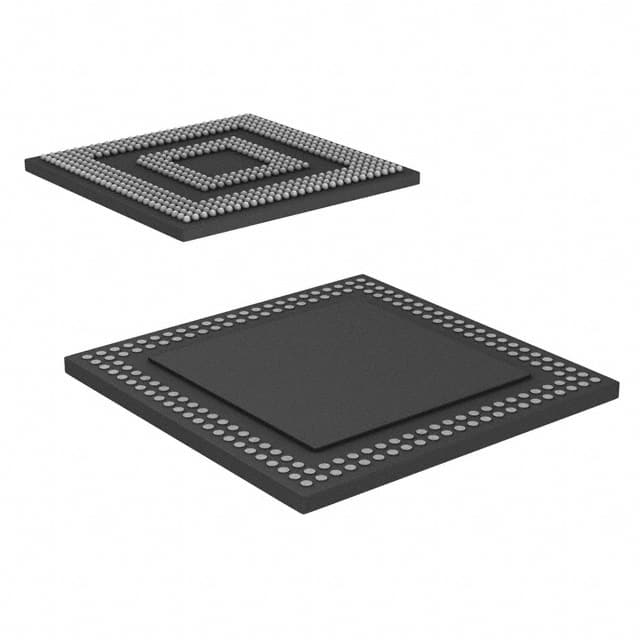
- Part No.:
- OMAP3530EZCBBA
- Manufacturer:
- Texas Instruments
- Category:
- Microprocessors
- Package:
- 515-VFBGA, FCBGA
- Datasheet:
-
 OMAP3530EZCBBA.pdf
- Description:
- IC MPU OMAP-35XX 600MHZ 515FCBGA
- Quantity:
- Payment:

- Shipping:

Inventory:1,937
Please send an inquiry. Send us your inquiry, and we will respond immediately.
Product details
Overview
OMAP3530EZCBBA from Texas Instruments is a high-reliability applications processor integrating an up to 600-MHz ARM Cortex-A8 MPU core, a 520-MHz TMS320C64x+ DSP core, and a POWERVR SGX graphics accelerator. It delivers hardware-accelerated video decode/encode (IVA2.2), real-time camera ISP, dual-display support (HD RGB + CVBS/S-Video), and programmable anti-aliasing - deployed in ruggedized portable navigation and digital video camera systems.
For engineers reviewing the OMAP3530EZCBBA datasheet, OMAP3530EZCBBA pinout, OMAP3530EZCBBA application, or OMAP3530EZCBBA equivalent, key selection criteria include its 515-pin s-PBGA (CBB) package with POP interface, SmartReflex™ adaptive voltage scaling, dual USB OTG/host subsystems, and discrete memory interface supporting LPDDR SDRAM and NAND/NOR flash with ECC.
Technical Context
The OMAP3530EZCBBA implements a heterogeneous multi-core architecture: the ARM Cortex-A8 executes Linux or Windows CE OS tasks with MMU and TrustZone security, while the C64x+ DSP handles real-time signal processing for imaging and audio. The IVA2.2 subsystem offloads H.264/MPEG-4 encode/decode, and the POWERVR SGX GPU provides tile-based rendering at up to 10 MPoly/sec.
Its memory subsystem includes 256 KB L2 cache, 64 KB shared SRAM, 112 KB ROM, and dual external interfaces - SDRC for LPDDR and GPMC for NAND/NOR/Flash/SRAM - all managed via L3/L4 interconnects. Power management uses SmartReflex AVS with dynamic voltage/frequency scaling across MPU, IVA, and core domains.
Key Specifications
| Parameter | Value and Actual Design Meaning |
|---|---|
| MPU Core | ARM Cortex-A8, up to 600 MHz - enables Linux kernel execution and application-level UI rendering with NEON SIMD acceleration. |
| DSP Core | TMS320C64x+, up to 520 MHz - performs real-time image signal processing, audio codecs, and video analytics in parallel with MPU. |
| Graphics Engine | POWERVR SGX (OMAP3530 only), 10 MPoly/sec - supports OpenGL ES 1.1/2.0 and OpenVG 1.0 for 3D UI and gaming effects. |
| Video Acceleration | IVA2.2 subsystem - hardware-accelerated H.264, MPEG-4, VC-1 decode/encode, plus preview/resizing/color space conversion. |
| Memory Interface | SDRC + GPMC - supports LPDDR SDRAM (up to 1 GByte) and NAND/NOR Flash with Hamming ECC, enabling boot-from-flash and low-power mobile memory. |
| Package | 515-pin s-PBGA (CBB suffix), 0.5 mm top / 0.4 mm bottom ball pitch - includes POP interface for stacked memory and discrete memory routing capability. |
| Operating Voltage | Adaptive core logic: 0.985–1.35 V - dynamically scaled via SmartReflex to minimize active power without performance loss. |
Pinout & Package
OMAP3530EZCBBA is housed in a 515-ball s-PBGA package (CBB suffix) with 0.5 mm ball pitch on top and 0.4 mm on bottom. The package supports Package-on-Package (POP) stacking and discrete memory interface routing. Pin assignments follow TI's CBB ball map (SPRS599D, Figures 2-1 through 2-5).
| Pin/Terminal | Circuit Role | Design Meaning |
|---|---|---|
| sdrc_d0–sdrc_d31 | SDRAM Data Bus | 32-bit bidirectional data path to LPDDR SDRAM; requires matched trace lengths and termination for DDR timing compliance. |
| sdrc_a0–sdrc_a14, sdrc_ba0–sdrc_ba1 | SDRAM Address & Bank Select | 16-bit address + 2-bit bank select for up to 1 GByte LPDDR addressing; controlled by SDRC scheduler. |
| gpmc_ncs0–gpmc_ncs7 | GPMC Chip Select | Eight independent chip selects for NOR/NAND/Flash/SRAM; gpmc_ncs1/ncs2 unavailable in CUS but present in CBB. |
| dss_data0–dss_data23, dss_hsync, dss_vsync | Display Subsystem Parallel Output | 24-bit RGB + sync signals for HD LCD panels; supports dual-panel output and RFBI interface for remote frame buffer. |
| cam_d0–cam_d11, cam_pclk, cam_vs, cam_hs | Camera ISP Parallel Input | 12-bit parallel CMOS/CCD sensor interface with pixel clock, vertical/horizontal sync - enables RAW capture at up to 1080p30. |
Key Features
| Feature | Design Value |
|---|---|
| SmartReflex™ AVS | Real-time adaptive voltage scaling across MPU, IVA, and core domains reduces active power by up to 40% vs. fixed-voltage operation. |
| IVA2.2 Hardware Acceleration | Offloads H.264 BP/MP decode (1080p30), encode (720p30), and JPEG encode/decode - frees CPU for application logic. |
| Camera ISP Pipeline | Integrated histogram, auto-exposure, auto-white balance, and auto-focus engines enable embedded vision without external co-processor. |
| POWERVR SGX Graphics | Programmable shader engine with OpenGL ES 2.0 support enables smooth 3D UI, gaming, and vector graphics on resource-constrained devices. |
| Dual USB Subsystem | Separate high-speed USB OTG (12-/8-pin ULPI) and multiport host controllers - supports simultaneous device/peripheral connectivity. |
Applications
| Portable Navigation Device (PND) | Digital Video Camera (DVC) |
|---|---|
Use Scenario: Ruggedized automotive-grade PND with turn-by-turn navigation, live traffic overlay, and voice guidance. IC Role / Device Role / Timing Role: Main applications processor executing Linux OS, rendering maps/UI, decoding traffic data streams, and driving TFT LCD + audio DAC. Use Value: Integrated IVA2.2 enables real-time map rendering + video overlay; SmartReflex extends battery life during GPS tracking. |
Use Scenario: High-definition handheld video camera recording 1080p30 H.264 video with optical zoom and electronic image stabilization. IC Role / Device Role / Timing Role: Central SoC handling sensor input (CMOS), real-time ISP processing, H.264 encoding, and SD card storage I/O. Use Value: On-die C64x+ DSP and IVA2.2 eliminate need for external encoder; dual-display output drives viewfinder + HDMI monitor simultaneously. |
| Advanced Portable Media Player (PMP) | Industrial Human-Machine Interface (HMI) |
Use Scenario: Secure, extended-temperature media player for field service tools with encrypted video playback and touchscreen UI. IC Role / Device Role / Timing Role: Applications processor running secure Linux, decrypting DRM-protected content, driving capacitive touchscreen and stereo audio. Use Value: TrustZone isolates secure media pipeline; POWERVR SGX renders fluid 3D menus; 188 GPIO support custom peripheral expansion. |
Use Scenario: Panel-mounted industrial HMI controlling PLCs, displaying real-time process data, and logging events to SD card. IC Role / Device Role / Timing Role: Deterministic real-time controller interfacing with RS-485, CAN (via external transceiver), and analog I/O modules. Use Value: Dual UARTs + McBSPs + McSPI enable legacy protocol bridging; watchdog timers and extended temp grade ensure uptime in harsh environments. |
Equivalent & Alternatives
The following parts are listed as comparable options for similar applications processor applications.
| Alternative Part | Technical Difference | Application Difference | Selection Advice |
|---|---|---|---|
| OMAP3525EZCBB | Lacks POWERVR SGX graphics accelerator and has no 3D rendering capability; identical MPU/DSP/ISP/USB/display subsystems. | Suitable for cost-sensitive PMP or DVC designs where 3D UI or gaming is not required. | Select when graphics acceleration is unnecessary and BOM cost reduction is prioritized over future UI scalability. |
| OMAP3530ECBB | Commercial-grade (non-HiRel) version; same silicon functionality but rated for 0°C to 90°C instead of extended temperature range. | Applicable in consumer electronics where extended temperature operation and radiation tolerance are not mandated. | Choose for non-mission-critical portable devices with standard environmental requirements and lower procurement cost. |
Compared with OMAP3525EZCBB, OMAP3530EZCBBA adds POWERVR SGX for OpenGL ES 2.0 rendering; compared with OMAP3530ECBB, it provides HiRel qualification for extended temperature (-40°C to 105°C) and enhanced reliability testing - critical for aerospace, defense, and industrial deployments.
Availability
OMAP3530EZCBBA is available at Aetrix Electronics and suitable for portable navigation devices, digital video cameras, and industrial HMIs requiring stable component supply across extended temperature ranges and long production lifecycles.
Supply support for OMAP3530EZCBBA includes scheduled delivery planning, volume procurement assistance, BOM continuity management, traceable sourcing, and lifecycle availability coordination for OEM customers, industrial embedded developers, connected-device designers, and electronics production programs.
Manufacturer
Texas Instruments is a global semiconductor leader specializing in analog, embedded processing, and wireless technologies, with decades of experience in high-reliability microprocessors and DSPs.
The OMAP3530 product line was designed for high-performance, low-power portable applications demanding integrated video, imaging, graphics, and real-time processing - targeting navigation, media, and industrial edge devices.
FAQ
What is the operating temperature range for OMAP3530EZCBBA?
The OMAP3530EZCBBA is a HiRel (high-reliability) variant qualified for operation from –40°C to +105°C ambient temperature. This extended range supports deployment in automotive under-hood, aerospace avionics, and industrial control environments where thermal stability is critical. The device incorporates enhanced screening and burn-in processes beyond commercial-grade OMAP3530ECBB.
Does OMAP3530EZCBBA support boot from NAND flash with ECC?
Yes, OMAP3530EZCBBA supports boot from NAND flash with built-in Hamming code ECC calculation via its General Purpose Memory Controller (GPMC). The GPMC handles ECC generation and correction transparently during boot and runtime, enabling reliable firmware storage without external ECC logic. This is confirmed in Section 2.5 and Table 1-1 of SPRS599D.
How many display outputs does OMAP3530EZCBBA support simultaneously?
OMAP3530EZCBBA supports two independent display outputs concurrently: one HD RGB interface (up to 24-bit, 1600×1200) and one composite/S-Video output (NTSC/PAL). Its dual-output 3-layer display processor allows overlaying graphics and video layers - for example, driving both a main LCD panel and a secondary CVBS monitor in digital signage or medical imaging systems.
What camera interfaces are available on OMAP3530EZCBBA?
OMAP3530EZCBBA integrates a dedicated Camera Image Signal Processor (ISP) with a 12-bit parallel interface supporting BT.601/BT.656 YCbCr 4:2:2 (8-/10-bit), RAW data input, and CCD/CMOS sensors. It includes full ISP pipeline features: histogram, auto-exposure, auto-white balance, auto-focus, resize, and color space conversion - all implemented in hardware without CPU load.
Is OMAP3530EZCBBA pin-compatible with OMAP3530ECBB?
Yes, OMAP3530EZCBBA and OMAP3530ECBB share identical pinout, package (515-pin s-PBGA CBB), and ball assignment per TI's SPRS599D documentation. Both use the same CBB mechanical footprint and electrical interface definitions - enabling drop-in replacement in commercial designs where HiRel qualification is not required.
OMAP3530EZCBBA Specifications
- Product attributes
- Attribute value
- Manufacturer:
- Texas Instruments
- Package/Case:
- 515-VFBGA, FCBGA
- Series:
- OMAP-35xx
- Packaging:
- Tray
- Product Status:
- Obsolete
- Core Processor:
- ARM® Cortex®-A8
- Number of Cores/Bus Width:
- 1 Core, 32-Bit
- Speed:
- 600MHz
- Co-Processors/DSP:
- Signal Processing; C64x+, Multimedia; NEON™ SIMD
- RAM Controllers:
- LPDDR
- Graphics Acceleration:
- Yes
- Display & Interface Controllers:
- LCD
- Ethernet:
- -
- SATA:
- -
- USB:
- USB 1.x (3), USB 2.0 (1)
- Voltage - I/O:
- 1.8V, 3.0V
- Operating Temperature:
- -40°C ~ 105°C (TJ)
- Grade:
- -
- Qualification:
- -
- Security Features:
- -
- Mounting Type:
- Surface Mount
- Supplier Device Package:
- 515-POP-FCBGA (12x12)
- Additional Interfaces:
- -
OMAP3530EZCBBA FAQ
1.How can I place an order for OMAP3530EZCBBA through Aetrix?
Please submit a Request for Quotation (RFQ) for OMAP3530EZCBBA on Aetrix. Our sales agent will provide a competitive quotation and guide you through the order confirmation once you accept the terms.
2.Are the price and stock information for OMAP3530EZCBBA reliable?
The price and inventory of OMAP3530EZCBBA are updated periodically and may fluctuate due to market conditions. Stock and pricing data are typically refreshed every 24 hours. Quotation validity for OMAP3530EZCBBA is usually 5 days.
3.What payment methods are accepted for OMAP3530EZCBBA?
We accept Wire Transfer, PayPal, Credit Card, Western Union, MoneyGram, and Escrow for OMAP3530EZCBBA transactions.
Note: Certain payment methods may incur a processing fee.
4.How is shipping managed for OMAP3530EZCBBA?
OMAP3530EZCBBA orders can be shipped via leading logistics carriers, including DHL, UPS, FedEx, TNT, or Registered Mail.
Once your OMAP3530EZCBBA order is processed, you will receive an email with the shipment details and tracking number.
Note: Tracking information may take up to 24 hours to appear. Express delivery typically takes 3–5 business days.
5.How can I obtain technical support or documentation for OMAP3530EZCBBA?
For technical support, including OMAP3530EZCBBA datasheets, pinout diagrams, or application guidance, please contact our engineering support team. They can provide detailed documentation and assistance for your OMAP3530EZCBBA requirements.
6.How does Aetrix verify that OMAP3530EZCBBA is sourced from the original manufacturer or authorized distributors?
All OMAP3530EZCBBA products on Aetrix are procured from qualified distributors and authorized channels. Our dedicated quality assurance team conducts strict verification, including traceability checks and, if necessary, third-party testing. This ensures that OMAP3530EZCBBA meets industry standards.
7.What is the process for return or replacement of OMAP3530EZCBBA?
All OMAP3530EZCBBA units undergo pre-shipment inspection (PSI). If there is an issue with OMAP3530EZCBBA, returns or replacements are accepted under the following conditions:
1.Quantity discrepancies, incorrect items, or visible external defects (such as breakage or corrosion), acknowledged by Aetrix.
2.The issue is reported within 90 days of delivery.
3.The OMAP3530EZCBBA part is unused and in its original packaging.
Return procedure for OMAP3530EZCBBA:
1.Submit a request within 90 days.
2.Obtain a Return Material Authorization (RMA) from Aetrix.
OMAP3530EZCBBA Tags

-
AT91SAM9260B-CU-999
Microchip Technology
-
AT91SAM9G25-CU
Microchip Technology

-
ATSAMA5D27C-CU
Microchip Technology
-
AT91SAM9X35-CU
Microchip Technology
-
AT91SAM9X25-CU
Microchip Technology

-
MCIMX6Y2CVM08AB
NXP Semiconductors
.JPG)
-
AM3352BZCZ100
Texas Instruments
-
AT91SAM9260B-CU
Microchip Technology

-
AT91SAM9260B-QU
Microchip Technology

-
ATSAMA5D31A-CU
Microchip Technology
-
AT91SAM9G20B-CU-999
Microchip Technology
-
MCIMX6Y2CVM05AB
NXP Semiconductors
Tech Hub

A practical engineering guide to 3.3V and 5V logic compatibility, input thresholds, resistor dividers, translator ICs, MOSFET level shifting, I2C pull-ups, timing limits and power-sequencing risks.

The 74HC595 uses push-pull logic outputs, while the TPIC6B595 uses 50 V open-drain DMOS sinks for higher-power loads. This guide compares timing, current limits, 3.3 V interfacing, load wiring, thermal…

The 74HC595 converts serial data into eight stable parallel outputs. This guide covers pin functions, shift and storage timing, OE and MR behavior, drive-current limits, cascading, voltage compatibilit…

A technical comparison of level-sensitive latches and edge-triggered flip-flops, covering timing windows, setup and hold limits, master–slave operation, time borrowing, race-through, HDL inference and…

A D latch stores one bit while Enable controls when data can pass. This reference covers gate-level operation, truth tables, transparency, setup and hold timing, LE versus OE, common ICs and practical …

An SR latch stores one bit through cross-coupled feedback. This engineering reference covers NOR and NAND implementations, truth tables, forbidden-state recovery, gated operation, switch debouncing, fa…

Latch circuits retain one bit through feedback. This technical reference covers SR and D latches, truth tables, transparency, timing limits, latch-versus-flip-flop behavior, applications and common log…

An engineering guide to LED driver operation, constant-current and constant-voltage outputs, linear and switching topologies, dimming, IC selection, calculations, replacement compatibility, and fault c…

Operational amplifier guide covering op amp basics, feedback, ideal vs real op amps, common configurations, buffer circuits, offset, bias current, gain-bandwidth, slew rate, rail-to-rail limits and sel…

Jumper cables guide covering safe connection order, red and black clamp placement, final ground connection, cable gauge, length, clamp quality, copper vs CCA cables, jump starter comparison and battery…


