
 My Inquiry
 My Account


Texas Instruments OMAPL132DZWTA2
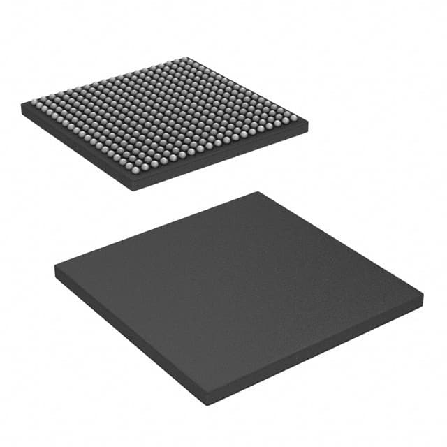
- Part No.:
- OMAPL132DZWTA2
- Manufacturer:
- Texas Instruments
- Category:
- Microprocessors
- Package:
- 361-LFBGA
- Datasheet:
-
 OMAPL132DZWTA2.pdf
- Description:
- IC MPU OMAP-L1X 200MHZ 361NFBGA
- Quantity:
- Payment:

- Shipping:

Inventory:4,537
Please send an inquiry. Send us your inquiry, and we will respond immediately.
Product details
Overview
OMAPL132DZWTA2 from Texas Instruments is a dual-core C6000™ DSP + ARM® applications processor integrating a 200-MHz ARM926EJ-S RISC MPU and a 200-MHz C674x fixed- and floating-point VLIW DSP. It delivers 1600 MIPS and 1200 MFLOPS, features 488KB on-chip RAM (including 256KB L2 unified RAM/cache), and supports DDR2/mDDR, EMIFA, USB 2.0 OTG, and 10/100 Ethernet - deployed in industrial portable navigation and smart grid substation protection systems.
For engineers reviewing the OMAPL132DZWTA2 datasheet, OMAPL132DZWTA2 pinout, OMAPL132DZWTA2 application, or OMAPL132DZWTA2 equivalent, key selection criteria include dual-core deterministic real-time processing, secure boot (AES-128/SHA-256), 128KB shared RAM for inter-processor communication, eHRPWM/eCAP timing peripherals, and PRUSS programmable real-time subsystem for offloading deterministic I/O tasks.
Technical Context
The OMAPL132DZWTA2 implements a tightly coupled heterogeneous architecture: the ARM926EJ-S core handles OS services, UI, and protocol stacks using its 16KB I-cache/16KB D-cache and MMU, while the C674x DSP executes compute-intensive signal processing with IEEE SP/DP floating-point support, 64 general-purpose registers, and dual multiply units enabling up to two SP×SP→SP operations per cycle.
Memory coherency is managed via shared 128KB SRAM and configurable L2 partitioning; peripheral access is coordinated through a high-performance switch fabric supporting EDMA3 (64 independent channels), dual McBSPs, McASP with 16 serializers, and PRUSS with two 32-bit RISC cores (4KB IRAM + 512B DRAM each) for hardware-timed GPIO, PWM, or custom protocol handling without CPU intervention.
Key Specifications
| Parameter | Value and Actual Design Meaning |
|---|---|
| CPU Cores | ARM926EJ-S @ 200 MHz + C674x DSP @ 200 MHz - enables concurrent OS execution and real-time signal processing without resource contention. |
| Performance | 1600 MIPS / 1200 MFLOPS - sufficient for multi-channel audio analysis, motor control algorithms, or biometric feature extraction in embedded edge devices. |
| On-Chip Memory | 488KB RAM total: 32KB L1P + 32KB L1D + 256KB L2 + 16KB I-Cache + 16KB D-Cache + 8KB vector RAM + 64KB ROM - eliminates need for external cache memory and reduces latency-critical accesses. |
| External Memory Support | DDR2/mDDR (16-bit, up to 156 MHz) + EMIFA (NOR/NAND/SDRAM) - allows flexible memory hierarchy: fast DDR2 for streaming buffers, NAND for firmware storage, SDRAM for legacy compatibility. |
| Security | AES-128 encryption + SHA-1/SHA-256 validation in Basic Secure Boot - protects boot image integrity and IP confidentiality; JTAG locked by default, unlocked only during authenticated development. |
| Real-Time Peripherals | 2× eHRPWM (6 dual-edge symmetric outputs each), 3× eCAP (32-bit timestamp capture), PRUSS (2× 32-bit RISC cores) - supports sub-microsecond I/O response for motor control, encoder interfacing, or custom serial protocols. |
| Connectivity | USB 2.0 OTG (integrated PHY), 10/100 EMAC (MII/RMII), 2× MMC/SD, 2× SPI, 2× I²C, 3× UART - enables full-featured HMI, field communication, and data logging without external bridge ICs. |
Pinout & Package
OMAPL132DZWTA2 is housed in a 361-ball Pb-free NFBGA (ZWT package) with 0.80-mm ball pitch and 16.0 mm × 16.0 mm body size. The package supports 1.2-V core and 1.8-V/3.3-V I/O operation, with dedicated power/ground ball arrays for noise-sensitive analog and digital domains.
| Pin/Terminal | Circuit Role | Design Meaning |
|---|---|---|
| VDD_CORE | Core Power Supply | 1.2-V nominal supply for ARM/DSP logic; requires low-noise regulation and local decoupling due to high transient current demands. |
| VDD_IO | I/O Power Supply | Selectable 1.8-V or 3.3-V rail for LVCMOS I/O banks; voltage must be set before configuration and maintained stable during operation. |
| CLKIN | Primary Clock Input | Accepts 24–30 MHz crystal or external clock; feeds PLLs generating core, DSP, and peripheral clocks - critical for timing accuracy and jitter-sensitive interfaces like USB/EMAC. |
| RESETn | Active-Low Reset Input | Synchronous deassertion required after power stabilization; initiates ARM/DSP cold boot sequence including ROM bootloader execution and memory initialization. |
| BOOT[3:0] | Boot Mode Configuration | 4-bit strap pins sampled at reset to select boot source (e.g., NAND, NOR, SPI flash, or UART); determines initial code fetch path and memory map layout. |
| EMU0/EMU1 | JTAG Emulation Interface | IEEE 1149.1 boundary-scan and debug interface; disabled by default in secure boot mode - requires explicit unlock via authenticated process. |
Key Features
| Feature | Design Value |
|---|---|
| Dual-core deterministic partitioning | ARM handles Linux/RTOS services and user interface; C674x DSP runs real-time signal processing - isolated memory maps and EDMA3 prevent interference. |
| PRUSS programmable I/O | Two independent 32-bit RISC cores with 4KB IRAM/512B DRAM each enable hardware-timed GPIO, PWM, quadrature decoding, or custom serial protocols without CPU overhead. |
| Secure boot with AES-128 | Encrypted boot image validated via SHA-256 before execution; prevents unauthorized firmware modification and ensures trusted execution from power-on. |
| eHRPWM with dead-band generation | 16-bit time-base counter with configurable period/frequency, 6 dual-edge symmetric outputs, and hardware trip-zone input - suitable for three-phase motor control with fault-safe shutdown. |
| EDMA3 with 64 channels | Two channel controllers and three transfer controllers enable zero-CPU-overhead data movement between peripherals (e.g., McASP → L2 RAM → DSP) and memory-to-memory transfers. |
| Flexible memory mapping | L2 RAM can be partitioned as cache, mapped RAM, or mixed; 128KB shared SRAM accessible by ARM, DSP, and EDMA3 - simplifies inter-processor communication and buffer sharing. |
Applications
| Industrial Portable Navigation Devices | Smart Grid Substation Protection |
|---|---|
Use Scenario: Rugged handheld units performing real-time GPS/INS fusion, map rendering, and wireless telemetry in utility field operations. IC Role / Device Role / Timing Role: OMAPL132DZWTA2 serves as main applications processor - ARM runs Linux-based HMI and comms stack; C674x executes Kalman filtering and sensor calibration algorithms. Use Value: Dual-core architecture enables simultaneous high-resolution display updates and sub-10ms sensor fusion loops without scheduling conflicts or latency spikes. |
Use Scenario: Intelligent electronic devices (IEDs) monitoring voltage/current waveforms, detecting faults, and executing tripping logic in high-voltage substations. IC Role / Device Role / Timing Role: OMAPL132DZWTA2 acts as protection controller - C674x performs real-time FFT and harmonic analysis on 16+ channel ADC streams; ARM manages SCADA reporting and human interface. Use Value: eCAP modules capture precise timestamped zero-crossings; PRUSS handles GOOSE message encoding with deterministic <5 µs latency - meeting IEC 61850-10 conformance requirements. |
| Biometric Identification Terminals | Professional Mobile Radio (PMR) Base Stations |
Use Scenario: Embedded fingerprint/vein recognition terminals used in access control, time & attendance, and identity verification at physical checkpoints. IC Role / Device Role / Timing Role: OMAPL132DZWTA2 functions as biometric engine - C674x accelerates image preprocessing, feature extraction, and template matching; ARM hosts secure enrollment database and TLS-secured cloud sync. Use Value: 128KB shared RAM enables rapid transfer of raw sensor frames to DSP; AES-128 secure boot ensures biometric templates cannot be extracted from compromised firmware images. |
Use Scenario: Digital trunked radio base stations implementing TETRA or DMR protocols with voice coding, channel equalization, and encryption in harsh RF environments. IC Role / Device Role / Timing Role: OMAPL132DZWTA2 operates as baseband processor - C674x executes AMBE+/MELP vocoders and adaptive equalizers; ARM manages network stack, remote management, and over-the-air updates. Use Value: McASP with 16 serializers supports full-duplex multichannel audio I/O; USB 2.0 OTG enables field technician firmware upgrades via standard flash drives - eliminating need for proprietary programming hardware. |
Equivalent & Alternatives
The following parts are listed as comparable options for similar dual-core DSP+ARM applications.
| Alternative Part | Technical Difference | Application Difference | Selection Advice |
|---|---|---|---|
| OMAPL138DZWTA2 | Same ZWT package but higher-speed 300-MHz ARM926EJ-S and C674x cores; adds 256KB additional L2 RAM (512KB total); identical peripheral set and pinout. | Required for applications needing >1600 MIPS or larger on-chip working memory for complex FFTs or multi-stream video analytics. | Select OMAPL138DZWTA2 when sustained computational throughput exceeds OMAPL132DZWTA2's 200-MHz limit, especially where L2 capacity bottlenecks occur in real-time buffering. |
| AM1808BZWT | ARM9-only variant (no C674x DSP); same 361-ball ZWT package, 200-MHz ARM926EJ-S, identical memory map and peripheral complement except DSP-specific blocks (L1P/L1D, EDMA3 enhancements, PRUSS). | Suitable for Linux-based HMI, gateway, or protocol translation where signal processing is handled externally or via software-only libraries. | Choose AM1808BZWT when DSP acceleration is unnecessary and cost reduction is prioritized - retains full ARM software compatibility and pin-for-pin layout reuse. |
Compared with OMAPL132DZWTA2, OMAPL138DZWTA2 offers higher clock speed and doubled L2 RAM for compute-bound workloads, while AM1808BZWT removes the DSP entirely to reduce BOM cost and power consumption - both maintain identical footprint, I/O compatibility, and software toolchain support.
Availability
OMAPL132DZWTA2 is available at Aetrix Electronics and suitable for industrial portable navigation devices, smart grid substation protection systems, biometric identification terminals, and professional mobile radio infrastructure requiring stable component supply across extended product lifecycles.
Supply support for OMAPL132DZWTA2 includes scheduled delivery planning, volume procurement assistance, BOM continuity management, traceable sourcing, and lifecycle availability coordination for OEM customers, industrial embedded developers, connected-device designers, and electronics production programs.
Manufacturer
Texas Instruments is a global semiconductor company headquartered in Dallas, Texas, delivering analog and embedded processing solutions for industrial, automotive, and communications markets since 1930.
The OMAP-L132 product line was designed for cost-sensitive, low-power industrial edge devices requiring deterministic real-time processing, secure firmware execution, and rich connectivity - bridging the gap between microcontrollers and high-end application processors.
FAQ
What is the maximum operating frequency of the ARM926EJ-S and C674x cores in OMAPL132DZWTA2?
The OMAPL132DZWTA2 integrates a 200-MHz ARM926EJ-S RISC processor and a 200-MHz C674x VLIW DSP core. Both operate at this rated frequency under recommended 1.2-V core supply and junction temperature conditions. This fixed-frequency specification is defined in the SPRS762E datasheet revision January 2017 and applies specifically to the OMAPL132DZWTA2 variant - not to higher-speed derivatives like OMAPL138DZWTA2.
Does OMAPL132DZWTA2 support secure boot, and what cryptographic algorithms are implemented?
Yes, OMAPL132DZWTA2 implements TI's Basic Secure Boot with hardware-enforced AES-128 encryption and SHA-1 or SHA-256 validation of boot images. The device uses a NIST-800-22 certified random number generator to derive a unique 128-bit cipher key, ensuring that encrypted firmware images can only be decrypted and authenticated by the target OMAPL132DZWTA2 unit - protecting intellectual property and preventing unauthorized code execution.
What external memory types does OMAPL132DZWTA2 support, and how are they interfaced?
OMAPL132DZWTA2 supports DDR2 SDRAM (16-bit, up to 156 MHz), mobile DDR (16-bit, up to 150 MHz), and asynchronous memories via EMIFA - including 8-/16-bit NOR flash, NAND flash, and 16-bit SDRAM. DDR2/mDDR connects through a dedicated high-speed controller with MRS register programming; EMIFA provides glueless interface to legacy parallel memories with configurable wait states and burst modes - both controllers are fully integrated and require no external logic.
Can the PRUSS on OMAPL132DZWTA2 be used independently of the ARM and DSP cores?
Yes, the Programmable Real-Time Unit Subsystem (PRUSS) on OMAPL132DZWTA2 consists of two independent 32-bit RISC cores, each with dedicated 4KB instruction RAM and 512 bytes of data RAM. It operates autonomously with its own clock domain and interrupt controller, and can be enabled or disabled via software without affecting ARM or DSP operation - enabling deterministic, low-latency I/O handling such as encoder counting or custom serial protocol generation without CPU scheduling delays.
What is the function of the 128KB shared RAM in OMAPL132DZWTA2, and how is it accessed?
The 128KB shared RAM in OMAPL132DZWTA2 is a dedicated on-chip SRAM block accessible by the ARM926EJ-S, C674x DSP, and EDMA3 controller via the internal switch fabric - without consuming L2 bandwidth. It serves as a zero-latency inter-processor communication buffer for passing sensor data, control commands, or processed results between ARM and DSP domains, and is mapped into both ARM and DSP address spaces at fixed physical addresses defined in the memory map.
OMAPL132DZWTA2 Specifications
- Product attributes
- Attribute value
- Manufacturer:
- Texas Instruments
- Package/Case:
- 361-LFBGA
- Series:
- OMAP-L1x
- Packaging:
- Tray
- Product Status:
- Obsolete
- Core Processor:
- ARM926EJ-S
- Number of Cores/Bus Width:
- 1 Core, 32-Bit
- Speed:
- 200MHz
- Co-Processors/DSP:
- Signal Processing; C674x, System Control; CP15
- RAM Controllers:
- LPDDR, DDR2
- Graphics Acceleration:
- No
- Display & Interface Controllers:
- -
- Ethernet:
- 10/100Mbps (1)
- SATA:
- -
- USB:
- USB 2.0 + PHY (1)
- Voltage - I/O:
- 1.8V, 3.3V
- Operating Temperature:
- -40°C ~ 105°C (TJ)
- Grade:
- -
- Qualification:
- -
- Security Features:
- -
- Mounting Type:
- Surface Mount
- Supplier Device Package:
- 361-NFBGA (16x16)
- Additional Interfaces:
- AC97, I2C, I2S, McASP, McBSP, MMC/SD/SDIO, SPI, UART
OMAPL132DZWTA2 FAQ
1.How can I place an order for OMAPL132DZWTA2 through Aetrix?
Please submit a Request for Quotation (RFQ) for OMAPL132DZWTA2 on Aetrix. Our sales agent will provide a competitive quotation and guide you through the order confirmation once you accept the terms.
2.Are the price and stock information for OMAPL132DZWTA2 reliable?
The price and inventory of OMAPL132DZWTA2 are updated periodically and may fluctuate due to market conditions. Stock and pricing data are typically refreshed every 24 hours. Quotation validity for OMAPL132DZWTA2 is usually 5 days.
3.What payment methods are accepted for OMAPL132DZWTA2?
We accept Wire Transfer, PayPal, Credit Card, Western Union, MoneyGram, and Escrow for OMAPL132DZWTA2 transactions.
Note: Certain payment methods may incur a processing fee.
4.How is shipping managed for OMAPL132DZWTA2?
OMAPL132DZWTA2 orders can be shipped via leading logistics carriers, including DHL, UPS, FedEx, TNT, or Registered Mail.
Once your OMAPL132DZWTA2 order is processed, you will receive an email with the shipment details and tracking number.
Note: Tracking information may take up to 24 hours to appear. Express delivery typically takes 3–5 business days.
5.How can I obtain technical support or documentation for OMAPL132DZWTA2?
For technical support, including OMAPL132DZWTA2 datasheets, pinout diagrams, or application guidance, please contact our engineering support team. They can provide detailed documentation and assistance for your OMAPL132DZWTA2 requirements.
6.How does Aetrix verify that OMAPL132DZWTA2 is sourced from the original manufacturer or authorized distributors?
All OMAPL132DZWTA2 products on Aetrix are procured from qualified distributors and authorized channels. Our dedicated quality assurance team conducts strict verification, including traceability checks and, if necessary, third-party testing. This ensures that OMAPL132DZWTA2 meets industry standards.
7.What is the process for return or replacement of OMAPL132DZWTA2?
All OMAPL132DZWTA2 units undergo pre-shipment inspection (PSI). If there is an issue with OMAPL132DZWTA2, returns or replacements are accepted under the following conditions:
1.Quantity discrepancies, incorrect items, or visible external defects (such as breakage or corrosion), acknowledged by Aetrix.
2.The issue is reported within 90 days of delivery.
3.The OMAPL132DZWTA2 part is unused and in its original packaging.
Return procedure for OMAPL132DZWTA2:
1.Submit a request within 90 days.
2.Obtain a Return Material Authorization (RMA) from Aetrix.
OMAPL132DZWTA2 Tags

-
AT91SAM9260B-CU-999
Microchip Technology
-
AT91SAM9G25-CU
Microchip Technology

-
ATSAMA5D27C-CU
Microchip Technology
-
AT91SAM9X35-CU
Microchip Technology
-
AT91SAM9X25-CU
Microchip Technology

-
MCIMX6Y2CVM08AB
NXP Semiconductors
.JPG)
-
AM3352BZCZ100
Texas Instruments
-
AT91SAM9260B-CU
Microchip Technology

-
AT91SAM9260B-QU
Microchip Technology

-
ATSAMA5D31A-CU
Microchip Technology
-
AT91SAM9G20B-CU-999
Microchip Technology
-
MCIMX6Y2CVM05AB
NXP Semiconductors
Tech Hub

A practical engineering guide to 3.3V and 5V logic compatibility, input thresholds, resistor dividers, translator ICs, MOSFET level shifting, I2C pull-ups, timing limits and power-sequencing risks.

The 74HC595 uses push-pull logic outputs, while the TPIC6B595 uses 50 V open-drain DMOS sinks for higher-power loads. This guide compares timing, current limits, 3.3 V interfacing, load wiring, thermal…

The 74HC595 converts serial data into eight stable parallel outputs. This guide covers pin functions, shift and storage timing, OE and MR behavior, drive-current limits, cascading, voltage compatibilit…

A technical comparison of level-sensitive latches and edge-triggered flip-flops, covering timing windows, setup and hold limits, master–slave operation, time borrowing, race-through, HDL inference and…

A D latch stores one bit while Enable controls when data can pass. This reference covers gate-level operation, truth tables, transparency, setup and hold timing, LE versus OE, common ICs and practical …

An SR latch stores one bit through cross-coupled feedback. This engineering reference covers NOR and NAND implementations, truth tables, forbidden-state recovery, gated operation, switch debouncing, fa…

Latch circuits retain one bit through feedback. This technical reference covers SR and D latches, truth tables, transparency, timing limits, latch-versus-flip-flop behavior, applications and common log…

An engineering guide to LED driver operation, constant-current and constant-voltage outputs, linear and switching topologies, dimming, IC selection, calculations, replacement compatibility, and fault c…

Operational amplifier guide covering op amp basics, feedback, ideal vs real op amps, common configurations, buffer circuits, offset, bias current, gain-bandwidth, slew rate, rail-to-rail limits and sel…

Jumper cables guide covering safe connection order, red and black clamp placement, final ground connection, cable gauge, length, clamp quality, copper vs CCA cables, jump starter comparison and battery…


