
 My Inquiry
 My Account


Texas Instruments OMAPL132EZWT2
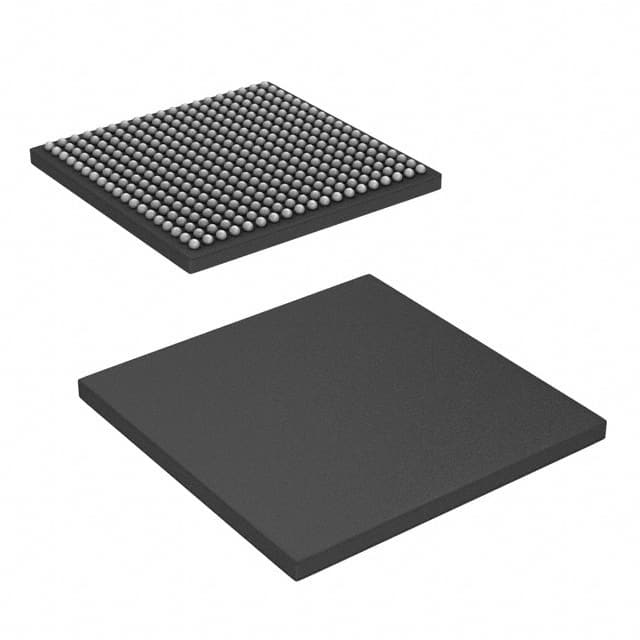
- Part No.:
- OMAPL132EZWT2
- Manufacturer:
- Texas Instruments
- Category:
- Microprocessors
- Package:
- 361-LFBGA
- Datasheet:
-
 OMAPL132EZWT2.pdf
- Description:
- IC MPU OMAP-L1X 200MHZ 361NFBGA
- Quantity:
- Payment:

- Shipping:

Inventory:3,465
Please send an inquiry. Send us your inquiry, and we will respond immediately.
Product details
Overview
OMAPL132EZWT2 from Texas Instruments is a dual-core C6000™ DSP + ARM® SoC integrating a 200-MHz ARM926EJ-S RISC MPU and a 200-MHz C674x fixed- and floating-point VLIW DSP. It delivers up to 1600 MIPS and 1200 MFLOPS, features 256KB L2 unified RAM/cache, 128KB shared SRAM, and supports DDR2/mDDR (16-bit, up to 156 MHz) for industrial embedded control and real-time signal processing.
For engineers reviewing the OMAPL132EZWT2 datasheet, OMAPL132EZWT2 pinout, OMAPL132EZWT2 application, or OMAPL132EZWT2 equivalent, key selection criteria include dual-core deterministic latency partitioning, secure boot with AES-128/SHA-256, EMAC+USB2.0 OTG+McASP peripheral integration, and 361-ball PBGA package compatibility with industrial thermal profiles.
Technical Context
The OMAPL132EZWT2 implements a tightly coupled ARM926EJ-S and C674x DSP subsystem sharing memory via a high-performance switch fabric, with separate 16KB I/D caches for ARM and 32KB L1P/L1D caches for DSP. Its EDMA3 controller provides 64 independent DMA channels and 16 QDMA channels for zero-overhead data movement between peripherals and L2/DDR2 memory.
Peripheral coherency is managed through configurable memory protection units (MPUs), while real-time determinism is enhanced by the PRUSS-two 32-bit RISC cores with 4KB instruction RAM each-operating independently of both CPU cores and supporting hardware-accelerated I/O timing critical for industrial PWM and capture functions.
Key Specifications
| Parameter | Value and Actual Design Meaning |
|---|---|
| CPU Architecture | Dual-core: ARM926EJ-S (200 MHz) + C674x VLIW DSP (200 MHz), enabling concurrent OS execution and real-time signal processing. |
| Memory Subsystem | 256KB L2 unified RAM/cache + 128KB shared SRAM + 16KB ARM I-cache/D-cache + 32KB DSP L1P/L1D - supports low-latency inter-processor communication without external DRAM dependency. |
| External Memory Support | 16-bit DDR2/mDDR (up to 156 MHz), EMIFA with NAND/NOR/SDRAM - enables cost-optimized BOM with single-channel high-bandwidth memory interface. |
| Connectivity Peripherals | 10/100 Mbps EMAC (MII/RMII), USB 2.0 OTG with integrated PHY, two McBSps, one McASP with 16 serializers - suitable for networked audio/video edge devices. |
| Real-Time I/O | Two eHRPWMs (6 single-edge or 6 dual-edge outputs with dead-band), three eCAP modules (32-bit timestamp capture), PRUSS with 2×4KB IRAM - meets sub-microsecond timing requirements in motor control and grid protection. |
| Security | Basic Secure Boot with AES-128 encryption, SHA-1/SHA-256 validation, JTAG lockdown - ensures trusted firmware execution and IP protection in field-deployed equipment. |
Pinout & Package
OMAPL132EZWT2 is housed in a 361-ball Pb-free NFBGA (ZWT suffix) with 0.80-mm ball pitch and 16.0 mm × 16.0 mm body size. The package supports industrial temperature range (–40°C to 105°C) and requires controlled PCB stack-up for signal integrity across high-speed DDR2 and USB interfaces.
| Pin/Terminal | Circuit Role | Design Meaning |
|---|---|---|
| VDD_CORE (multiple) | Core power supply | 1.2-V nominal supply for ARM926EJ-S and C674x DSP cores; decoupling required per TI layout guidelines to maintain voltage stability under dynamic load. |
| VDD_IO (multiple) | I/O power supply | Configurable 1.8-V or 3.3-V LVCMOS I/O bank supply; allows mixed-voltage interfacing with legacy peripherals without level shifters. |
| CLKIN | Primary clock input | Accepts 32.768-kHz crystal or external oscillator for RTC and system PLL reference; supports frequency multiplication to generate core clocks. |
| EMAC_MDIO / EMAC_MDC | Ethernet management interface | Provides bidirectional configuration and status access to external PHY; essential for auto-negotiation and link monitoring in industrial Ethernet nodes. |
| USB0_DP / USB0_DM | USB 2.0 differential pair | Integrated PHY eliminates need for external transceiver; supports host/client modes and high/full-speed operation with on-chip termination. |
| DDR2_DQ[15:0] | Data bus | 16-bit bidirectional DDR2 data interface; routed with matched length and controlled impedance for reliable 156-MHz operation. |
Key Features
| Feature | Design Value |
|---|---|
| Dual-core asymmetric multiprocessing | ARM926EJ-S handles Linux/RTOS tasks and UI, while C674x DSP offloads intensive math (FFT, filtering, codec); cache-coherent memory map avoids software-managed data copies. |
| PRUSS programmable I/O subsystem | Two independent 32-bit RISC cores with dedicated 4KB IRAM each enable cycle-accurate GPIO, PWM, and protocol emulation without CPU intervention - ideal for time-critical industrial I/O. |
| EDMA3 with 64-channel arbitration | Hardware-managed data transfers between peripherals (McASP, EMAC, DDR2) and memory eliminate CPU overhead and guarantee deterministic latency for streaming applications. |
| Secure boot with AES-128/SHA-256 | Root-of-trust execution starts from encrypted, authenticated boot image stored in external flash; prevents unauthorized firmware modification in deployed smart grid or biometric systems. |
| Flexible memory mapping and protection | MPUs allow per-peripheral and per-memory-region access control by ARM, DSP, or PRUSS - enforces functional safety isolation between safety-critical and non-safety partitions. |
Applications
| Industrial Motor Control | Smart Grid Protection Relay |
|---|---|
|
Use Scenario: Closed-loop servo drive with field-oriented control (FOC) and real-time fault detection. IC Role / Device Role / Timing Role: OMAPL132EZWT2 executes FOC algorithm on C674x DSP while ARM9 manages HMI and EtherCAT stack; eHRPWM outputs drive gate drivers with <100-ns dead-band precision. Use Value: Dual-core deterministic scheduling ensures 50-µs current loop update without jitter, meeting IEC 61800-7 functional safety timing constraints. |
Use Scenario: Substation relay performing real-time harmonic analysis, distance protection, and GOOSE messaging. IC Role / Device Role / Timing Role: C674x DSP computes FFT-based harmonic distortion and impedance trajectories; ARM9 runs IEC 61850 stack and stores event logs in DDR2. Use Value: 1200 MFLOPS enables 64-point FFT in <20 µs, satisfying IEEE C37.118 synchrophasor latency requirements for Class P compliance. |
| Biometric Identification Terminal | Professional Mobile Radio (PMR) Base Station |
|
Use Scenario: Fingerprint/face recognition terminal with secure template storage and wireless upload. IC Role / Device Role / Timing Role: ARM9 hosts Linux OS and TLS-secured Wi-Fi stack; C674x DSP performs real-time fingerprint matching and AES-256 template encryption. Use Value: On-chip 128KB shared SRAM buffers biometric images without external memory access, reducing power and attack surface for secure enrollment. |
Use Scenario: TETRA or DMR base station handling multi-channel voice encoding, RF synchronization, and network backhaul. IC Role / Device Role / Timing Role: McASP interfaces with audio codecs; eCAP captures precise RF timing markers; EMAC routes VoIP packets over fiber/Ethernet. Use Value: Integrated McASP with DIT capability and 16 serializers supports simultaneous 8-channel TDM voice streams with <1-µs channel alignment. |
Equivalent & Alternatives
The following parts are listed as comparable options for similar dual-core DSP+ARM applications.
| Alternative Part | Technical Difference | Application Difference | Selection Advice |
|---|---|---|---|
| OMAPL138EZWT2 | Higher 300-MHz C674x DSP clock, 512KB L2 RAM, same ZWT package - adds 50% compute headroom but increases power draw by ~25% at full load. | Targeted at higher-throughput audio analytics and multi-stream video encode where OMAPL132EZWT2 reaches CPU saturation. | Select OMAPL138EZWT2 only when application requires >1600 MIPS sustained performance and can accommodate higher thermal design power. |
| AM1808BZWT2 | ARM9-only (no DSP core), 456-MHz ARM926EJ-S, identical peripheral set except no C674x, PRUSS, or L2 cache - lower cost and power, but lacks hardware-accelerated signal processing. | Suitable for HMI-centric industrial controllers where real-time math is handled externally or via software libraries. | Choose AM1808BZWT2 when DSP offload is unnecessary and BOM cost reduction is prioritized over computational density. |
Compared with OMAPL132EZWT2, OMAPL138EZWT2 offers higher DSP throughput at increased power, while AM1808BZWT2 removes the DSP entirely to reduce cost and complexity - making OMAPL132EZWT2 the optimal balance of real-time signal processing, peripheral richness, and thermal efficiency for mid-tier industrial edge devices.
Availability
OMAPL132EZWT2 is available at Aetrix Electronics and suitable for industrial automation, smart grid protection relays, biometric identification terminals, and professional mobile radio infrastructure requiring stable component supply across extended product lifecycles.
Supply support for OMAPL132EZWT2 includes scheduled delivery planning, volume procurement assistance, BOM continuity management, traceable sourcing, and lifecycle availability coordination for OEM customers, industrial embedded developers, connected-device designers, and electronics production programs.
Manufacturer
Texas Instruments is a global semiconductor company specializing in analog, embedded processing, and connectivity technologies, with leadership in industrial, automotive, and communications markets.
The OMAP-L132 product line was designed for cost-sensitive, power-constrained industrial edge applications requiring deterministic real-time processing, secure boot, and rich peripheral integration - bridging the gap between microcontrollers and high-end application processors.
FAQ
What is the maximum DDR2 clock frequency supported by OMAPL132EZWT2?
OMAPL132EZWT2 supports DDR2 operation up to 156 MHz, corresponding to 312 MT/s data rate on its 16-bit bus. This is specified in the device's electrical characteristics table and validated across commercial and extended temperature ranges. The DDR2 controller includes programmable timing parameters and on-die termination calibration to ensure signal integrity at this speed. Designers must follow TI's layout guidelines for trace length matching and power delivery to achieve stable operation.
Does OMAPL132EZWT2 include hardware encryption acceleration?
OMAPL132EZWT2 does not integrate a dedicated cryptographic accelerator engine. However, it supports Basic Secure Boot using AES-128 for image decryption and SHA-1/SHA-256 for signature validation - implemented in ROM-based boot code. For runtime encryption, developers leverage the C674x DSP's optimized instruction set or ARM9's software libraries. No hardware AES/SHA engines are present on-die; all crypto operations rely on CPU execution or external co-processors.
Can the PRUSS on OMAPL132EZWT2 be used for Ethernet packet processing?
Yes, the PRUSS on OMAPL132EZWT2 can handle time-critical Ethernet frame preprocessing - such as VLAN tagging, checksum offload, or real-time timestamp insertion - before passing packets to the EMAC. Each PRU has direct access to EMAC registers and shared memory, enabling sub-microsecond response to packet events. However, full TCP/IP stack processing remains on the ARM9; PRUSS is best suited for deterministic, low-level packet manipulation that must occur outside the OS scheduler.
What debug interfaces are available on OMAPL132EZWT2?
OMAPL132EZWT2 provides JTAG (IEEE 1149.1) for boundary scan and core debugging, plus an Embedded Trace Buffer (ETB) with 4KB capacity for ARM9 instruction tracing. The JTAG port is locked by default in secure boot mode but can be enabled during development. No SWD or cJTAG interface is supported. Debug access requires TI's XDS100v3 or XDS200 emulators and Code Composer Studio v5.x or later for full visibility into both ARM and DSP execution contexts.
Is OMAPL132EZWT2 pin-compatible with other OMAP-L13x variants?
OMAPL132EZWT2 shares the same 361-ball ZWT package and pinout with OMAPL137EZWT2 and OMAPL138EZWT2, enabling drop-in replacement within the same family. Key signals - including DDR2, EMAC, USB, McASP, and power domains - are identically mapped. However, differences in internal memory size (e.g., L2 RAM), clock speeds, and feature enablement require firmware and bootloader updates to fully utilize upgraded variants or maintain compatibility with downgraded ones.
OMAPL132EZWT2 Specifications
- Product attributes
- Attribute value
- Manufacturer:
- Texas Instruments
- Package/Case:
- 361-LFBGA
- Series:
- OMAP-L1x
- Packaging:
- Tray
- Product Status:
- Active
- Core Processor:
- ARM926EJ-S
- Number of Cores/Bus Width:
- 1 Core, 32-Bit
- Speed:
- 200MHz
- Co-Processors/DSP:
- Signal Processing; C674x, System Control; CP15
- RAM Controllers:
- LPDDR, DDR2
- Graphics Acceleration:
- No
- Display & Interface Controllers:
- -
- Ethernet:
- 10/100Mbps (1)
- SATA:
- -
- USB:
- USB 2.0 + PHY (1)
- Voltage - I/O:
- 1.8V, 3.3V
- Operating Temperature:
- 0°C ~ 90°C (TJ)
- Grade:
- -
- Qualification:
- -
- Security Features:
- -
- Mounting Type:
- Surface Mount
- Supplier Device Package:
- 361-NFBGA (16x16)
- Additional Interfaces:
- AC97, I2C, I2S, McASP, McBSP, MMC/SD/SDIO, SPI, UART
OMAPL132EZWT2 FAQ
1.How can I place an order for OMAPL132EZWT2 through Aetrix?
Please submit a Request for Quotation (RFQ) for OMAPL132EZWT2 on Aetrix. Our sales agent will provide a competitive quotation and guide you through the order confirmation once you accept the terms.
2.Are the price and stock information for OMAPL132EZWT2 reliable?
The price and inventory of OMAPL132EZWT2 are updated periodically and may fluctuate due to market conditions. Stock and pricing data are typically refreshed every 24 hours. Quotation validity for OMAPL132EZWT2 is usually 5 days.
3.What payment methods are accepted for OMAPL132EZWT2?
We accept Wire Transfer, PayPal, Credit Card, Western Union, MoneyGram, and Escrow for OMAPL132EZWT2 transactions.
Note: Certain payment methods may incur a processing fee.
4.How is shipping managed for OMAPL132EZWT2?
OMAPL132EZWT2 orders can be shipped via leading logistics carriers, including DHL, UPS, FedEx, TNT, or Registered Mail.
Once your OMAPL132EZWT2 order is processed, you will receive an email with the shipment details and tracking number.
Note: Tracking information may take up to 24 hours to appear. Express delivery typically takes 3–5 business days.
5.How can I obtain technical support or documentation for OMAPL132EZWT2?
For technical support, including OMAPL132EZWT2 datasheets, pinout diagrams, or application guidance, please contact our engineering support team. They can provide detailed documentation and assistance for your OMAPL132EZWT2 requirements.
6.How does Aetrix verify that OMAPL132EZWT2 is sourced from the original manufacturer or authorized distributors?
All OMAPL132EZWT2 products on Aetrix are procured from qualified distributors and authorized channels. Our dedicated quality assurance team conducts strict verification, including traceability checks and, if necessary, third-party testing. This ensures that OMAPL132EZWT2 meets industry standards.
7.What is the process for return or replacement of OMAPL132EZWT2?
All OMAPL132EZWT2 units undergo pre-shipment inspection (PSI). If there is an issue with OMAPL132EZWT2, returns or replacements are accepted under the following conditions:
1.Quantity discrepancies, incorrect items, or visible external defects (such as breakage or corrosion), acknowledged by Aetrix.
2.The issue is reported within 90 days of delivery.
3.The OMAPL132EZWT2 part is unused and in its original packaging.
Return procedure for OMAPL132EZWT2:
1.Submit a request within 90 days.
2.Obtain a Return Material Authorization (RMA) from Aetrix.
OMAPL132EZWT2 Tags

-
AT91SAM9260B-CU-999
Microchip Technology
-
AT91SAM9G25-CU
Microchip Technology

-
ATSAMA5D27C-CU
Microchip Technology
-
AT91SAM9X35-CU
Microchip Technology
-
AT91SAM9X25-CU
Microchip Technology

-
MCIMX6Y2CVM08AB
NXP Semiconductors
.JPG)
-
AM3352BZCZ100
Texas Instruments
-
AT91SAM9260B-CU
Microchip Technology

-
AT91SAM9260B-QU
Microchip Technology

-
ATSAMA5D31A-CU
Microchip Technology
-
AT91SAM9G20B-CU-999
Microchip Technology
-
MCIMX6Y2CVM05AB
NXP Semiconductors
Tech Hub

A practical engineering guide to 3.3V and 5V logic compatibility, input thresholds, resistor dividers, translator ICs, MOSFET level shifting, I2C pull-ups, timing limits and power-sequencing risks.

The 74HC595 uses push-pull logic outputs, while the TPIC6B595 uses 50 V open-drain DMOS sinks for higher-power loads. This guide compares timing, current limits, 3.3 V interfacing, load wiring, thermal…

The 74HC595 converts serial data into eight stable parallel outputs. This guide covers pin functions, shift and storage timing, OE and MR behavior, drive-current limits, cascading, voltage compatibilit…

A technical comparison of level-sensitive latches and edge-triggered flip-flops, covering timing windows, setup and hold limits, master–slave operation, time borrowing, race-through, HDL inference and…

A D latch stores one bit while Enable controls when data can pass. This reference covers gate-level operation, truth tables, transparency, setup and hold timing, LE versus OE, common ICs and practical …

An SR latch stores one bit through cross-coupled feedback. This engineering reference covers NOR and NAND implementations, truth tables, forbidden-state recovery, gated operation, switch debouncing, fa…

Latch circuits retain one bit through feedback. This technical reference covers SR and D latches, truth tables, transparency, timing limits, latch-versus-flip-flop behavior, applications and common log…

An engineering guide to LED driver operation, constant-current and constant-voltage outputs, linear and switching topologies, dimming, IC selection, calculations, replacement compatibility, and fault c…

Operational amplifier guide covering op amp basics, feedback, ideal vs real op amps, common configurations, buffer circuits, offset, bias current, gain-bandwidth, slew rate, rail-to-rail limits and sel…

Jumper cables guide covering safe connection order, red and black clamp placement, final ground connection, cable gauge, length, clamp quality, copper vs CCA cables, jump starter comparison and battery…


