
 My Inquiry
 My Account


Texas Instruments OMAPL138EZWTA3E
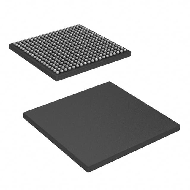
- Part No.:
- OMAPL138EZWTA3E
- Manufacturer:
- Texas Instruments
- Category:
- Microprocessors
- Package:
- 361-LFBGA
- Datasheet:
-
 OMAPL138EZWTA3E.pdf
- Description:
- IC MPU OMAP-L1X 375MHZ 361NFBGA
- Quantity:
- Payment:

- Shipping:

Inventory:2,153
Please send an inquiry. Send us your inquiry, and we will respond immediately.
Product details
Overview
OMAPL138EZWTA3E from Texas Instruments is a dual-core C6000™ DSP + ARM® SoC integrating a 456-MHz ARM926EJ-S RISC MPU and a 456-MHz C674x VLIW DSP, with 256KB L2 unified RAM/cache, 128KB shared RAM, and 1.8-/3.3-V LVCMOS I/Os - deployed in industrial portable navigation, smart grid substation protection, and biometric identification systems.
For engineers reviewing the OMAPL138EZWTA3E datasheet, OMAPL138EZWTA3E pinout, OMAPL138EZWTA3E application, or OMAPL138EZWTA3E equivalent, key selection considerations include dual-core clock synchronization, DDR2/mDDR memory controller timing compliance, EMAC MII/RMII interface configuration, and PRUSS real-time peripheral offload capability.
Technical Context
The OMAPL138EZWTA3E implements a tightly coupled ARM926EJ-S and C674x DSP subsystem sharing L2 memory and EDMA3 resources, with independent cache hierarchies (16KB I-cache/16KB D-cache for ARM; 32KB L1P/32KB L1D for DSP) and hardware-assisted cache coherency management. Its memory architecture supports concurrent access to 256KB L2 RAM/cache and 128KB dedicated shared RAM without performance contention.
Peripheral interconnect uses a multi-layer AHB/AXI fabric enabling simultaneous high-bandwidth transfers across EMAC, SATA, uPP, and VPIF - with programmable pin multiplexing allowing dynamic allocation of 361-ball PBGA terminals between McASP, McBSP, USB OTG/Host, and dual SPI/MMC interfaces under system-level timing constraints.
Key Specifications
| Parameter | Value and Actual Design Meaning |
|---|---|
| CPU Frequency | 456 MHz ARM926EJ-S and 456 MHz C674x DSP at 1.3V core supply - enables deterministic real-time processing with <1.2 µs interrupt latency for safety-critical control loops. |
| L2 Memory | 256KB unified mapped RAM/cache - configurable as full RAM, full cache, or partitioned; accessible by both ARM and DSP without arbitration stalls. |
| Shared RAM | 128KB dedicated on-chip RAM - isolated from DSP L2 to guarantee deterministic bandwidth for ARM-side OS services and UI rendering. |
| External Memory | DDR2/mDDR controller (16-bit, 256MB address space) + EMIFA (NOR/NAND/SDRAM) - supports boot-from-NAND and dual-memory-boot redundancy. |
| Security | TI Basic Secure Boot with AES-128 encryption and SHA-256 validation - protects boot image integrity and prevents unauthorized firmware execution via JTAG lockdown. |
| USB Interfaces | USB 2.0 OTG (high/full/low-speed) + USB 1.1 OHCI host - enables field-upgradable firmware delivery and peripheral attachment without external hub logic. |
| Real-Time Peripherals | PRUSS with two 32-bit RISC cores (4KB IRAM + 512B DRAM each), eHRPWM (6 dual-edge outputs), eCAP (32-bit timestamp capture) - offloads deterministic I/O timing from main CPUs. |
Pinout & Package
OMAPL138EZWTA3E is housed in a 361-ball NFBGA package (ZWT suffix) with 16.0 mm × 16.0 mm body size and 0.80-mm ball pitch, compliant with JEDEC MO-256. Thermal pad exposed on underside requires solder paste stencil design per TI SZZA031.
| Pin/Terminal | Circuit Role | Design Meaning |
|---|---|---|
| CLKIN | Oscillator Input | Accepts 24–48 MHz crystal or LVCMOS clock; feeds PLL1 for ARM/DSP core clocks and PLL2 for peripheral clocks. |
| VDD_CORE | Core Power Supply | 1.3V ±3% supply for 456-MHz operation; requires low-ESR ceramic decoupling within 3 mm of ball array. |
| VDD_IO | I/O Power Supply | Configurable 1.8V or 3.3V supply; sets voltage level for all LVCMOS I/O banks except USB/DDR2 interfaces. |
| EMIF_A[18:0] | EMIFA Address Bus | 19-bit multiplexed address for NOR/NAND/SDRAM; timing controlled by EMIF_ACFG register group with programmable setup/hold cycles. |
| DDR2_DQ[15:0] | DDR2 Data Bus | 16-bit bidirectional data lane; requires matched trace length (±5 mm) and on-die termination calibration via ZQ pin during initialization. |
| USB0_DP/DM | USB 2.0 OTG Differential Pair | Integrated PHY supports high-speed (480 Mbps) signaling; requires 90-Ω differential impedance and 3.3V VBUS detection circuitry. |
| PRU0_R30 | PRUSS Exported Register | Direct-accessible 32-bit register from PRU0 core; used for real-time GPIO control or status handshake with ARM subsystem. |
Key Features
| Feature | Design Value |
|---|---|
| Dual-core cache coherency | Hardware-managed L1/L2 cache consistency between ARM and DSP via shared memory mapping - eliminates software cache-flush overhead in inter-processor communication. |
| Programmable Real-Time Unit Subsystem | Two independent 32-bit PRU cores with dedicated instruction/data RAM - executes deterministic I/O tasks (e.g., encoder quadrature decoding, PWM dead-band insertion) without CPU intervention. |
| Secure boot enforcement | AES-128 decryption and SHA-256 hash validation applied to boot image before execution - prevents runtime injection of malicious code into ROM-resident bootloader. |
| Flexible memory interface | EMIFA + DDR2/mDDR controllers support simultaneous boot-from-NAND and application execution from DDR2 - enables fail-safe firmware recovery without external flash controller. |
| High-speed parallel I/O | uPP interface with 8–16-bit programmable data width and dual-data-rate mode - achieves >100 MB/s throughput to FPGAs or ADCs without PCIe complexity. |
Applications
| Industrial Portable Navigation Devices | Smart Grid Substation Protection |
|---|---|
Use Scenario: Ruggedized handheld units performing real-time GPS/INS fusion, map rendering, and voice-guided routing in field maintenance operations. IC Role / Device Role / Timing Role: OMAPL138EZWTA3E serves as central applications processor executing Linux-based navigation stack while offloading sensor fusion math to C674x DSP and managing display/audio via LCD controller and McASP. Use Value: Dual-core architecture delivers 2746 MFLOPS DSP compute for Kalman filtering plus ARM926EJ-S UI responsiveness - enabling sub-100ms route recalculation under moving vehicle conditions. | Use Scenario: IEDs monitoring power line current/voltage waveforms and triggering breaker trips within 2 ms of fault detection in 110 kV substations. IC Role / Device Role / Timing Role: OMAPL138EZWTA3E acts as protection algorithm engine, acquiring analog inputs via McBSP-connected ADCs, executing harmonic analysis on C674x DSP, and issuing trip commands through eHRPWM-controlled solid-state relays. Use Value: PRUSS real-time peripherals execute cycle-accurate waveform sampling and zero-crossing detection - meeting IEC 61850-10 Class T3 timing requirements without RTOS jitter. |
| Biometric Identification Terminals | Remote Radio Head (RRH) Baseband Processing |
Use Scenario: Embedded fingerprint/vein scanners verifying identity at physical access points with local template storage and anti-spoofing liveness detection. IC Role / Device Role / Timing Role: OMAPL138EZWTA3E functions as secure biometric coprocessor: ARM handles encrypted template matching and TLS-secured enrollment upload; C674x DSP performs real-time image preprocessing and feature extraction. Use Value: TI Basic Secure Boot ensures cryptographic keys remain inaccessible during boot - preventing physical extraction of stored biometric templates from NAND flash. | Use Scenario: Outdoor RRH units digitizing RF signals from antenna arrays and performing baseband modulation/demodulation for LTE-TDD small cells. IC Role / Device Role / Timing Role: OMAPL138EZWTA3E operates as baseband processor: C674x DSP executes FFT/IFFT, channel estimation, and LDPC decoding; ARM manages CPRI interface, OAM messaging, and thermal throttling. Use Value: SATA controller enables local recording of IQ samples for field diagnostics; EMAC+MDIO provides backhaul connectivity to BBU with IEEE 1588 timestamping support. |
Equivalent & Alternatives
The following parts are listed as comparable options for similar dual-core DSP+ARM applications.
| Alternative Part | Technical Difference | Application Difference | Selection Advice |
|---|---|---|---|
| OMAPL138CZCEA3 | Same die, 361-ball 0.65-mm pitch PBGA (ZCE), 375-MHz max frequency, 1.2V core - lower thermal density but reduced compute throughput. | Suitable for cost-sensitive industrial HMIs where 456-MHz deterministic latency is not required. | Select when PCB layout prioritizes smaller footprint (13×13 mm) over peak performance. |
| AM3358BZCZ100 | ARM Cortex-A8 single-core (1 GHz), no integrated DSP, PRU-ICSS instead of PRUSS, lacks SATA and McASP - higher ARM IPC but no native floating-point acceleration. | Better for Linux-based gateway applications with heavy TCP/IP stack load but minimal signal processing. | Choose when application demands Gigabit Ethernet, USB 2.0 host, and industrial protocol stacks over DSP-accelerated math. |
Compared with OMAPL138EZWTA3E, OMAPL138CZCEA3 trades 21% lower clock rate and smaller package for reduced thermal design complexity, while AM3358BZCZ100 abandons DSP hardware entirely in favor of higher single-thread ARM performance and broader Linux driver support - making it viable only where C674x-specific algorithms are absent.
Availability
OMAPL138EZWTA3E is available at Aetrix Electronics and suitable for industrial portable navigation devices, smart grid substation protection IEDs, and biometric identification terminals requiring stable component supply across extended product lifecycles.
Supply support for OMAPL138EZWTA3E includes scheduled delivery planning, volume procurement assistance, BOM continuity management, traceable sourcing, and lifecycle availability coordination for OEM customers, industrial embedded developers, connected-device designers, and electronics production programs.
Manufacturer
Texas Instruments is a global semiconductor company headquartered in Dallas, Texas, delivering analog and embedded processing solutions for industrial, automotive, and communications markets since 1930.
The OMAP-L138 product line was engineered to bridge high-performance DSP computation with ARM-based OS capabilities in resource-constrained industrial edge devices - targeting applications demanding both real-time signal processing and rich user interfaces.
FAQ
What is the maximum operating frequency of the OMAPL138EZWTA3E and what voltage is required?
The OMAPL138EZWTA3E operates at a maximum frequency of 456 MHz for both its ARM926EJ-S and C674x DSP cores, requiring a 1.3V ±3% core supply (VDD_CORE) as specified in the SPRS586J datasheet Section 5.3. This voltage level is mandatory to sustain 456-MHz operation; using 1.2V limits maximum frequency to 375 MHz. The OMAPL138EZWTA3E's power management unit dynamically adjusts core voltage during DVFS transitions to maintain stability.
Does the OMAPL138EZWTA3E support secure boot, and what cryptographic algorithms are implemented?
Yes, the OMAPL138EZWTA3E implements TI Basic Secure Boot using AES-128 for boot image encryption and SHA-256 for image authentication, as documented in the TMS320C674x/OMAP-L1x Processor Security User's Guide. The secure boot flow begins from a hardware root-of-trust, locks JTAG by default, and decrypts/authenticates images loaded from external NAND or SPI flash. OMAPL138EZWTA3E does not support RSA or ECC-based signature verification - only symmetric AES/SHA primitives.
What memory interfaces are available on the OMAPL138EZWTA3E and how are they allocated?
The OMAPL138EZWTA3E integrates two independent memory controllers: a DDR2/mDDR controller supporting 16-bit bus width and 256MB address space, and an EMIFA supporting 8/16-bit NOR/NAND flash and 16-bit SDRAM. These interfaces are electrically isolated and managed by separate AHB masters. The OMAPL138EZWTA3E also includes 256KB of on-chip L2 RAM/cache and 128KB of dedicated shared RAM - all accessible without arbitration delay.
How does the PRUSS subsystem in the OMAPL138EZWTA3E differ from standard microcontroller peripherals?
The PRUSS in the OMAPL138EZWTA3E contains two independent 32-bit RISC cores (PRU0/PRU1), each with 4KB instruction RAM and 512B data RAM, executing at full core clock speed without cache or MMU - enabling sub-microsecond I/O response. Unlike standard peripherals, PRUSS exposes register R30 for direct ARM-DSP-PRU handshaking and supports real-time GPIO, PWM, and encoder functions without CPU scheduling. OMAPL138EZWTA3E's PRUSS is disabled by default and must be enabled via PSC registers.
What USB configurations does the OMAPL138EZWTA3E support and are external PHYs required?
The OMAPL138EZWTA3E integrates two USB PHYs: a USB 2.0 OTG PHY (USB0) supporting high/full/low-speed device/host modes, and a USB 1.1 OHCI PHY (USB1) for full-speed host-only operation. No external PHYs are required - both interfaces use internal transceivers with on-die termination. The OMAPL138EZWTA3E's USB0 port complies with USB 2.0 specification and supports up to four endpoints (control, bulk, interrupt, isochronous) with hardware-assisted descriptor handling.
OMAPL138EZWTA3E Specifications
- Product attributes
- Attribute value
- Manufacturer:
- Texas Instruments
- Package/Case:
- 361-LFBGA
- Series:
- OMAP-L1x
- Packaging:
- Tray
- Product Status:
- Active
- Core Processor:
- ARM926EJ-S
- Number of Cores/Bus Width:
- 1 Core, 32-Bit
- Speed:
- 375MHz
- Co-Processors/DSP:
- Signal Processing; C674x, System Control; CP15
- RAM Controllers:
- SDRAM
- Graphics Acceleration:
- No
- Display & Interface Controllers:
- LCD
- Ethernet:
- 10/100Mbps (1)
- SATA:
- SATA 3Gbps (1)
- USB:
- USB 1.1 + PHY (1), USB 2.0 + PHY (1)
- Voltage - I/O:
- 1.8V, 3.3V
- Operating Temperature:
- -40°C ~ 105°C (TJ)
- Grade:
- -
- Qualification:
- -
- Security Features:
- Boot Security, Cryptography
- Mounting Type:
- Surface Mount
- Supplier Device Package:
- 361-NFBGA (16x16)
- Additional Interfaces:
- HPI, I2C, McASP, McBSP, MMC/SD, SPI, UART
OMAPL138EZWTA3E FAQ
1.How can I place an order for OMAPL138EZWTA3E through Aetrix?
Please submit a Request for Quotation (RFQ) for OMAPL138EZWTA3E on Aetrix. Our sales agent will provide a competitive quotation and guide you through the order confirmation once you accept the terms.
2.Are the price and stock information for OMAPL138EZWTA3E reliable?
The price and inventory of OMAPL138EZWTA3E are updated periodically and may fluctuate due to market conditions. Stock and pricing data are typically refreshed every 24 hours. Quotation validity for OMAPL138EZWTA3E is usually 5 days.
3.What payment methods are accepted for OMAPL138EZWTA3E?
We accept Wire Transfer, PayPal, Credit Card, Western Union, MoneyGram, and Escrow for OMAPL138EZWTA3E transactions.
Note: Certain payment methods may incur a processing fee.
4.How is shipping managed for OMAPL138EZWTA3E?
OMAPL138EZWTA3E orders can be shipped via leading logistics carriers, including DHL, UPS, FedEx, TNT, or Registered Mail.
Once your OMAPL138EZWTA3E order is processed, you will receive an email with the shipment details and tracking number.
Note: Tracking information may take up to 24 hours to appear. Express delivery typically takes 3–5 business days.
5.How can I obtain technical support or documentation for OMAPL138EZWTA3E?
For technical support, including OMAPL138EZWTA3E datasheets, pinout diagrams, or application guidance, please contact our engineering support team. They can provide detailed documentation and assistance for your OMAPL138EZWTA3E requirements.
6.How does Aetrix verify that OMAPL138EZWTA3E is sourced from the original manufacturer or authorized distributors?
All OMAPL138EZWTA3E products on Aetrix are procured from qualified distributors and authorized channels. Our dedicated quality assurance team conducts strict verification, including traceability checks and, if necessary, third-party testing. This ensures that OMAPL138EZWTA3E meets industry standards.
7.What is the process for return or replacement of OMAPL138EZWTA3E?
All OMAPL138EZWTA3E units undergo pre-shipment inspection (PSI). If there is an issue with OMAPL138EZWTA3E, returns or replacements are accepted under the following conditions:
1.Quantity discrepancies, incorrect items, or visible external defects (such as breakage or corrosion), acknowledged by Aetrix.
2.The issue is reported within 90 days of delivery.
3.The OMAPL138EZWTA3E part is unused and in its original packaging.
Return procedure for OMAPL138EZWTA3E:
1.Submit a request within 90 days.
2.Obtain a Return Material Authorization (RMA) from Aetrix.
OMAPL138EZWTA3E Tags

-
AT91SAM9260B-CU-999
Microchip Technology
-
AT91SAM9G25-CU
Microchip Technology

-
ATSAMA5D27C-CU
Microchip Technology
-
AT91SAM9X35-CU
Microchip Technology
-
AT91SAM9X25-CU
Microchip Technology

-
MCIMX6Y2CVM08AB
NXP Semiconductors
.JPG)
-
AM3352BZCZ100
Texas Instruments
-
AT91SAM9260B-CU
Microchip Technology

-
AT91SAM9260B-QU
Microchip Technology

-
ATSAMA5D31A-CU
Microchip Technology
-
AT91SAM9G20B-CU-999
Microchip Technology
-
MCIMX6Y2CVM05AB
NXP Semiconductors
Tech Hub

A practical engineering guide to 3.3V and 5V logic compatibility, input thresholds, resistor dividers, translator ICs, MOSFET level shifting, I2C pull-ups, timing limits and power-sequencing risks.

The 74HC595 uses push-pull logic outputs, while the TPIC6B595 uses 50 V open-drain DMOS sinks for higher-power loads. This guide compares timing, current limits, 3.3 V interfacing, load wiring, thermal…

The 74HC595 converts serial data into eight stable parallel outputs. This guide covers pin functions, shift and storage timing, OE and MR behavior, drive-current limits, cascading, voltage compatibilit…

A technical comparison of level-sensitive latches and edge-triggered flip-flops, covering timing windows, setup and hold limits, master–slave operation, time borrowing, race-through, HDL inference and…

A D latch stores one bit while Enable controls when data can pass. This reference covers gate-level operation, truth tables, transparency, setup and hold timing, LE versus OE, common ICs and practical …

An SR latch stores one bit through cross-coupled feedback. This engineering reference covers NOR and NAND implementations, truth tables, forbidden-state recovery, gated operation, switch debouncing, fa…

Latch circuits retain one bit through feedback. This technical reference covers SR and D latches, truth tables, transparency, timing limits, latch-versus-flip-flop behavior, applications and common log…

An engineering guide to LED driver operation, constant-current and constant-voltage outputs, linear and switching topologies, dimming, IC selection, calculations, replacement compatibility, and fault c…

Operational amplifier guide covering op amp basics, feedback, ideal vs real op amps, common configurations, buffer circuits, offset, bias current, gain-bandwidth, slew rate, rail-to-rail limits and sel…

Jumper cables guide covering safe connection order, red and black clamp placement, final ground connection, cable gauge, length, clamp quality, copper vs CCA cables, jump starter comparison and battery…


