
 My Inquiry
 My Account


Texas Instruments ONET1131ECRSMT
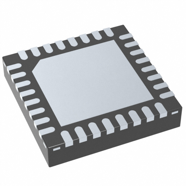
- Part No.:
- ONET1131ECRSMT
- Manufacturer:
- Texas Instruments
- Category:
- Audio Special Purpose
- Package:
- 32-VFQFN Exposed Pad
- Datasheet:
-
 ONET1131ECRSMT.pdf
- Description:
- IC MODULATOR 32VQFN
- Quantity:
- Payment:

- Shipping:

Inventory:1,357
Please send an inquiry. Send us your inquiry, and we will respond immediately.
Product details
Overview
ONET1131ECRSMT from Texas Instruments is a 2.5-V externally modulated laser driver IC with integrated reference-free clock and data recovery (CDR), supporting 9.8–11.7 Gbps operation, delivering up to 150 mA bias current for EML/MZM lasers, and featuring programmable input equalization, cross-point control, and de-emphasis for optical eye margin optimization in 10-Gbps PON OLT and SFP+/XFP transceivers.
For engineers reviewing the ONET1131ECRSMT datasheet, ONET1131ECRSMT pinout, ONET1131ECRSMT application, or ONET1131ECRSMT equivalent, this device serves as a single-chip CDR + modulator driver solution requiring no external reference clock, enabling compact, low-power, high-reliability optical transmitter designs compliant with CPRI, SONET OC-192, 10GBASE-ER/ZR, and Fibre Channel standards.
Technical Context
The ONET1131ECRSMT implements a fully integrated transmit path comprising an adjustable 4-tap CTLE equalizer (supporting up to 300 mm FR4 trace loss), a multi-rate reference-free CDR with programmable jitter transfer bandwidth (8 MHz typical at 9.95 Gbps), and a CML output modulator driver configurable for single-ended (2 Vpp max) or differential (3.6 Vpp max) operation. It embeds closed-loop APC using photodiode feedback with selectable monitor ranges (0.75–3 µA/step) and real-time diagnostics via on-chip ADCs for supply voltage, temperature, bias current, and PD current.
Control is executed via a 2-wire digital interface (400 kHz max SCK) with integrated DACs/ADCs, enabling full configuration of output polarity, CDR bypass mode, transmit equalization, de-emphasis (5–6 dB), and laser safety features including fault detection (FLT), loss-of-lock (LOL), and bias disable (DIS) with 100 ns reset pulse requirement. All analog monitoring pins (MONB, MONP, AMP, LF, COMP) are functionally validated per TI SLLSEQ6A Rev A.
Key Specifications
| Parameter | Value and Actual Design Meaning |
|---|---|
| Data Rate | 9.8–11.7 Gbps reference-free CDR operation; supports lower rates via CDR bypass mode. |
| Bias Current Range | 5–150 mA source (EML/MZM); programmable via DAC with ±15% DMI accuracy. |
| Output Amplitude | Up to 2 Vpp single-ended or 3.6 Vpp differential into 50 Ω / 100 Ω loads; amplitude stability ±230 mVpp. |
| Input Equalization | Configurable CTLE supporting up to 300 mm FR4 microstrip/stripline; 6–9 dB boost at 7 GHz. |
| Jitter Performance | 60 mUIpp total jitter generation (BER = 10⁻¹²); 0.4–0.75 psRMS random jitter; <5 ps ISI with EQ enabled. |
| Supply & Temp | Single 2.5 V ±5% supply; operates from –40°C to +100°C ambient; thermal pad RθJB = 7.8 °C/W. |
| Diagnostics | Integrated ADCs monitor VCC (±2%), temperature (±3°C), I(BIAS) (±15%), I(PD) (±15%), with 12-bit resolution. |
Pinout & Package
ONET1131ECRSMT is housed in a RoHS-compliant 4 mm × 4 mm, 32-pin VQFN package (RSM) with 0.4 mm pitch and exposed thermal pad. Pin functions are electrically validated per TI SLLSEQ6A Rev A; all NC pins (20, 21, 24, 25, 26, 28, 29) must remain unconnected.
| Pin/Terminal | Circuit Role | Design Meaning |
|---|---|---|
| 1 LOL | Digital output | Open-drain loss-of-lock indicator; requires 4.7–10 kΩ pull-up to VCC; 3.3 V tolerant. |
| 2 MONB | Analog output | Bias current monitor (1% ratio); used for APC loop feedback and fault detection (VMONB-FLT = 1.2 V). |
| 4 DIN+ | Analog input | Non-inverted CML data input; on-chip 100 Ω differential termination; AC-coupled only. |
| 5 DIN− | Analog input | Inverted CML data input; complements DIN+; matched termination ensures common-mode rejection. |
| 7 PD | Analog input | Photodiode current input for APC loop; reverse-biased up to 2.3 V; fault threshold set via TXPMF register. |
| 8 MONP | Analog output | Photodiode current monitor (10–60% ratio depending on TXPDRNG setting); enables closed-loop power control. |
| 9 LF | Analog input | Transmitter loop filter capacitor connection; sets APC loop dynamics (0.01 µF to ground). |
| 10 BIAS | Analog I/O | Laser bias current sink/source node; compliance voltage ≥0.45 V (sink) or ≤VCC − 0.45 V (source). |
| 11,14,27,30 VCC | Power supply | 2.5 V ±5% analog supply for modulator driver and CDR; multiple pins reduce IR drop and noise. |
| 12 OUT− | CML output | Inverted differential output; internally terminated in single-ended mode; drives EML/MZM cathode/anode. |
| 13 OUT+ | CML output | Non-inverted differential output; paired with OUT−; supports cross-point adjustment (35–75%). |
| 15 VDD | Power supply | 2.5 V ±5% digital supply for 2-wire interface, registers, and control logic; isolated from analog VCC. |
| 16 AMP | Analog input | Amplitude control voltage input (0–2 V); sets output swing without digital register access. |
| 17 SDA | Digital I/O | 2-wire serial data line; open-drain, 3.3 V tolerant; requires external 4.7–10 kΩ pull-up to VCC. |
| 18 SCK | Digital input | 2-wire serial clock input; 400 kHz max; 3.3 V tolerant; requires same pull-up as SDA. |
| 31 FLT | Digital output | Open-drain fault flag; asserts high on APC error, overtemp, supply fault, or bias/PD monitor violation. |
| 32 DIS | Digital input | Bias disable control; internal 250 kΩ pull-up; 100 ns high pulse resets FLT/LOL; ORed with TXBIASEN bit. |
Key Features
| Feature | Design Value |
|---|---|
| Reference-free CDR | Eliminates need for external clock source across 9.8–11.7 Gbps; reduces board space and jitter accumulation. |
| Programmable APC loop | Compensates optical power drift over temperature/voltage/time using user-selectable PD monitor range (0.75–3 µA/step). |
| Transmit waveform shaping | Cross-point (35–75%) and de-emphasis (5–6 dB) optimize optical eye mask margin for long-haul fiber links. |
| Integrated diagnostics | On-chip ADCs report real-time VCC, temperature, I(BIAS), and I(PD) - enabling SFF-8472-compliant digital diagnostics. |
| Laser safety architecture | Dual-fault detection (FLT + LOL), bias disable (DIS), and photodiode monitor fault thresholds prevent laser damage during startup/failure. |
Applications
| 10-Gbps PON OLT Transceiver | XFP/SFP+ 10GBASE-ER/ZR Module |
|---|---|
Use Scenario: Optical Line Terminal in FTTx passive optical networks transmitting downstream data over 20–60 km single-mode fiber. IC Role / Device Role / Timing Role: Laser driver + CDR retimer for EML-based transmitter; provides precise bias control and jitter-cleaned clock/data to laser. Use Value: Enables stable 10-Gbps transmission under wide temperature variation (–40°C to +100°C) with automatic optical power regulation per ITU-T G.987/G.984. |
Use Scenario: Long-reach Ethernet optical module for data center interconnects requiring 40 km (ER) or 80 km (ZR) reach over SMF. IC Role / Device Role / Timing Role: Reference-free CDR + modulator driver in XFP/SFP+ form factor; recovers and retimes degraded electrical signals before optical modulation. Use Value: Meets IEEE 802.3ae 10GBASE-ER/ZR jitter specs with <60 mUIpp total jitter generation and supports MSA-compliant diagnostics via 2-wire interface. |
| SONET OC-192 Transmitter | 8x/10x Fibre Channel Optical Link |
Use Scenario: Telecom backbone equipment transmitting synchronous optical network traffic at 9.953 Gbps (OC-192). IC Role / Device Role / Timing Role: High-stability CDR + EML driver ensuring strict SONET jitter transfer (GR-253-CORE) and mask compliance. Use Value: Jitter transfer bandwidth of 8 MHz at 9.95 Gbps meets SONET requirements; integrated APC maintains average optical power within ±0.5 dB. |
Use Scenario: Storage area network switch or HBA transmitting 8.5 Gbps (8x) or 10.5 Gbps (10x) Fibre Channel over multimode/single-mode fiber. IC Role / Device Role / Timing Role: Retiming modulator driver for FC-PI-4/FC-PI-5 transmitters; equalizes channel loss and shapes optical eye for BER <10⁻¹². Use Value: Input equalization supports up to 300 mm FR4 traces; deterministic jitter <8 psPP ensures FC-PI-5 eye compliance at 10.5 Gbps. |
Equivalent & Alternatives
The following parts are listed as comparable options for similar laser driver + CDR applications.
| Alternative Part | Technical Difference | Application Difference | Selection Advice |
|---|---|---|---|
| MAX3736AETE+ | Supports 10–11.3 Gbps; no integrated APC loop; requires external photodiode monitor circuit; 3.3 V supply only. | Targeted at cost-sensitive short-reach modules where closed-loop power control is not required. | Select when APC is unnecessary and system-level photodiode monitoring is already implemented. |
| LMH1218RTVT | 12.5 Gbps max; includes integrated TIA for receiver path; no built-in CDR; requires external clock for retiming. | Designed for bidirectional SFP+ modules needing both Tx driver and Rx TIA in one package. | Choose only if dual-path integration (Tx + Rx) is needed and external CDR is acceptable. |
Compared with MAX3736AETE+ and LMH1218RTVT, the ONET1131ECRSMT uniquely integrates reference-free CDR, closed-loop APC, and full diagnostic ADCs in a single 2.5 V, 32-pin QFN - reducing BOM count and enabling compact, standards-compliant 10-Gbps optical transmitters without external timing or power control components.
Availability
ONET1131ECRSMT is available at Aetrix Electronics and suitable for 10-Gbps PON OLT systems, XFP/SFP+ 10GBASE-ER/ZR modules, and SONET OC-192 optical transceivers requiring stable component supply, long-lifecycle support, and guaranteed traceable sourcing.
Supply support for ONET1131ECRSMT includes scheduled delivery planning, volume procurement assistance, BOM continuity management, traceable sourcing, and lifecycle availability coordination for OEM customers, industrial embedded developers, connected-device designers, and electronics production programs.
Manufacturer
Texas Instruments is a global semiconductor leader specializing in analog, embedded processing, and connectivity technologies for industrial, automotive, and communications infrastructure markets.
The ONET1131ECRSMT belongs to TI's ONET family of optical networking ICs, designed specifically for high-speed, low-power, standards-compliant optical transmitter subsystems in access and metro networks.
FAQ
What is the primary function of the ONET1131ECRSMT in an optical transceiver?
The ONET1131ECRSMT serves as an integrated externally modulated laser driver with reference-free clock and data recovery (CDR), providing bias current control, input equalization, output waveform shaping, and closed-loop automatic power control (APC) for EML and MZM lasers. Its core role is to condition and drive high-speed electrical data into a clean, jitter-controlled optical signal - making it essential for 10-Gbps PON OLT, XFP/SFP+, and SONET OC-192 transmitters. The ONET1131ECRSMT eliminates the need for external clock sources and discrete APC circuitry.
Does the ONET1131ECRSMT require an external reference clock for CDR operation?
No, the ONET1131ECRSMT features a reference-free CDR architecture that locks and recovers clock and data autonomously across 9.8–11.7 Gbps without any external clock input. This capability is confirmed in the datasheet (SLLSEQ6A Rev A, Section 3) and enables simplified board design, reduced jitter accumulation, and compliance with standards like CPRI and 10GBASE-ER that prohibit external clock dependencies. The ONET1131ECRSMT also supports CDR bypass mode for lower data rates.
How does the APC loop in the ONET1131ECRSMT maintain stable optical output power?
The ONET1131ECRSMT implements a closed-loop APC system that monitors photodiode current (via PD and MONP pins), compares it to a user-defined target, and dynamically adjusts laser bias current (via BIAS pin) to maintain constant average optical power. It supports three selectable monitor ranges (0.75/1.5/3 µA per step), includes a dedicated loop filter pin (LF), and achieves ±0.5 dB average power stability over voltage, temperature, and aging - all documented in Section 6.5 and Figure 7 of the ONET1131ECRSMT datasheet.
Can the ONET1131ECRSMT be used with both EML and MZM lasers?
Yes, the ONET1131ECRSMT is explicitly designed to support externally modulated lasers including Electro-Absorption Modulator (EML) lasers and Mach-Zehnder Modulator (MZM) lasers, as stated in the "Features" section (page 1) and "Description" (page 1) of the official TI datasheet SLLSEQ6A. Its output driver delivers up to 150 mA bias current with configurable polarity (BIASPOL register), and its CML outputs (OUT+/OUT−) provide the high-swing, low-jitter drive required by both EML and MZM architectures.
What package type and thermal characteristics does the ONET1131ECRSMT have?
The ONET1131ECRSMT uses a 4 mm × 4 mm, 32-pin VQFN (RSM) package with 0.4 mm pitch and an exposed thermal pad. Its thermal performance is characterized by RθJB = 7.8 °C/W (junction-to-board) and RθJA = 37.2 °C/W (junction-to-ambient), enabling reliable operation from –40°C to +100°C ambient. The package is RoHS-compliant and optimized for high-density optical module layouts - details are specified in Section 6.4 and Mechanical Information (Section 12) of the ONET1131ECRSMT datasheet.
ONET1131ECRSMT Specifications
- Product attributes
- Attribute value
- Manufacturer:
- Texas Instruments
- Series:
- -
- Package/Case:
- 32-VFQFN Exposed Pad
- Packaging:
- Tape & Reel (TR)
- Product Status:
- Active
- Function:
- Modulator
- Applications:
- Driver
- Number of Channels:
- 2
- Interface:
- I2C
- Voltage - Supply:
- 2.37V ~ 2.63V
- Operating Temperature:
- -40°C ~ 100°C (TA)
- Specifications:
- -
- Mounting Type:
- Surface Mount
- Grade:
- -
ONET1131ECRSMT FAQ
1.How can I place an order for ONET1131ECRSMT through Aetrix?
Please submit a Request for Quotation (RFQ) for ONET1131ECRSMT on Aetrix. Our sales agent will provide a competitive quotation and guide you through the order confirmation once you accept the terms.
2.Are the price and stock information for ONET1131ECRSMT reliable?
The price and inventory of ONET1131ECRSMT are updated periodically and may fluctuate due to market conditions. Stock and pricing data are typically refreshed every 24 hours. Quotation validity for ONET1131ECRSMT is usually 5 days.
3.What payment methods are accepted for ONET1131ECRSMT?
We accept Wire Transfer, PayPal, Credit Card, Western Union, MoneyGram, and Escrow for ONET1131ECRSMT transactions.
Note: Certain payment methods may incur a processing fee.
4.How is shipping managed for ONET1131ECRSMT?
ONET1131ECRSMT orders can be shipped via leading logistics carriers, including DHL, UPS, FedEx, TNT, or Registered Mail.
Once your ONET1131ECRSMT order is processed, you will receive an email with the shipment details and tracking number.
Note: Tracking information may take up to 24 hours to appear. Express delivery typically takes 3–5 business days.
5.How can I obtain technical support or documentation for ONET1131ECRSMT?
For technical support, including ONET1131ECRSMT datasheets, pinout diagrams, or application guidance, please contact our engineering support team. They can provide detailed documentation and assistance for your ONET1131ECRSMT requirements.
6.How does Aetrix verify that ONET1131ECRSMT is sourced from the original manufacturer or authorized distributors?
All ONET1131ECRSMT products on Aetrix are procured from qualified distributors and authorized channels. Our dedicated quality assurance team conducts strict verification, including traceability checks and, if necessary, third-party testing. This ensures that ONET1131ECRSMT meets industry standards.
7.What is the process for return or replacement of ONET1131ECRSMT?
All ONET1131ECRSMT units undergo pre-shipment inspection (PSI). If there is an issue with ONET1131ECRSMT, returns or replacements are accepted under the following conditions:
1.Quantity discrepancies, incorrect items, or visible external defects (such as breakage or corrosion), acknowledged by Aetrix.
2.The issue is reported within 90 days of delivery.
3.The ONET1131ECRSMT part is unused and in its original packaging.
Return procedure for ONET1131ECRSMT:
1.Submit a request within 90 days.
2.Obtain a Return Material Authorization (RMA) from Aetrix.
ONET1131ECRSMT Tags

-
SA571DR2G
onsemi
-
ADAU7002ACBZ-R7
Analog Devices Inc.

-
DRV135UA/2K5
Texas Instruments

-
DRV134UA/1K
Texas Instruments

-
DRV134PA
Texas Instruments
-
DRV134UA
Texas Instruments
-
DRV135UA
Texas Instruments
-
SA572DR2G
onsemi
-
PGA2311U/1K
Texas Instruments
-
SI8244BB-D-IS1R
Skyworks Solutions Inc.

-
CS8416K-CZZR
Cirrus Logic Inc.
-
SRC4392IPFBR
Texas Instruments
Tech Hub

A practical engineering guide to 3.3V and 5V logic compatibility, input thresholds, resistor dividers, translator ICs, MOSFET level shifting, I2C pull-ups, timing limits and power-sequencing risks.

The 74HC595 uses push-pull logic outputs, while the TPIC6B595 uses 50 V open-drain DMOS sinks for higher-power loads. This guide compares timing, current limits, 3.3 V interfacing, load wiring, thermal…

The 74HC595 converts serial data into eight stable parallel outputs. This guide covers pin functions, shift and storage timing, OE and MR behavior, drive-current limits, cascading, voltage compatibilit…

A technical comparison of level-sensitive latches and edge-triggered flip-flops, covering timing windows, setup and hold limits, master–slave operation, time borrowing, race-through, HDL inference and…

A D latch stores one bit while Enable controls when data can pass. This reference covers gate-level operation, truth tables, transparency, setup and hold timing, LE versus OE, common ICs and practical …

An SR latch stores one bit through cross-coupled feedback. This engineering reference covers NOR and NAND implementations, truth tables, forbidden-state recovery, gated operation, switch debouncing, fa…

Latch circuits retain one bit through feedback. This technical reference covers SR and D latches, truth tables, transparency, timing limits, latch-versus-flip-flop behavior, applications and common log…

An engineering guide to LED driver operation, constant-current and constant-voltage outputs, linear and switching topologies, dimming, IC selection, calculations, replacement compatibility, and fault c…

Operational amplifier guide covering op amp basics, feedback, ideal vs real op amps, common configurations, buffer circuits, offset, bias current, gain-bandwidth, slew rate, rail-to-rail limits and sel…

Jumper cables guide covering safe connection order, red and black clamp placement, final ground connection, cable gauge, length, clamp quality, copper vs CCA cables, jump starter comparison and battery…


