
 My Inquiry
 My Account


Texas Instruments ONET4291PARGVR
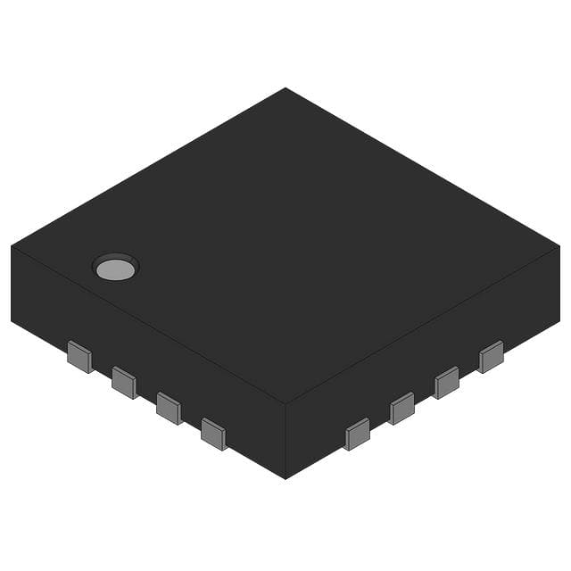
- Part No.:
- ONET4291PARGVR
- Manufacturer:
- Texas Instruments
- Category:
- Instrumentation, Op Amps, Buffer Amps
- Package:
- 16-VQFN Exposed Pad
- Datasheet:
-
 ONET4291PARGVR.pdf
- Description:
- IC LIMITING 1 CIRCUIT 16VQFN
- Quantity:
- Payment:

- Shipping:

Inventory:3,728
Please send an inquiry. Send us your inquiry, and we will respond immediately.
Product details
Overview
ONET4291PARGVR from Texas Instruments is a 1-Gbps to 4.25-Gbps rate-selectable limiting amplifier with CML differential outputs, on-chip 50-Ω back-termination to VCC, and integrated loss-of-signal (LOS) detection. It delivers ~43 dB gain, supports digital bandwidth/output amplitude/LOS threshold control via two-wire interface, and operates from a single 3.3-V supply in –40°C to 85°C ambient.
For engineers reviewing the ONET4291PARGVR datasheet, ONET4291PARGVR pinout, ONET4291PARGVR application, or ONET4291PARGVR equivalent, this device serves as a high-speed front-end amplifier in fiber-optic receiver chains requiring programmable sensitivity, jitter-tolerant signal recovery, and multirate SONET/SDH, Fibre Channel, and Gigabit Ethernet compliance.
Technical Context
The ONET4291PARGVR implements a high-speed data path with DC feedback for input offset cancellation, using dual gain stages (37 dB + 6 dB) and a CML output buffer. Its digitally controlled bandwidth switch supports 16 discrete settings from 0.73 GHz to 4.39 GHz, directly mapping to data rates up to 4.25 Gbps.
Loss-of-signal detection uses dual peak detectors monitoring first- and second-stage outputs, comparing against a programmable threshold set either by external resistor (TH-to-GND) or internal 6-bit digitally selectable resistor (RTHI, 8–86.75 kΩ). The two-wire interface (SCK/SDA) enables register-based configuration of bandwidth (4-bit), output amplitude (2-bit), and LOS threshold (6-bit).
Key Specifications
| Parameter | Value and Actual Design Meaning |
|---|---|
| Data rate range | 1.0625 Gbps, 2.125 Gbps, and 4.25 Gbps - matches standard Fibre Channel, Gigabit Ethernet, and SONET OC-48/SDH STM-16 line rates. |
| Small-signal gain | 38–46 dB - ensures full CML output swing (400–1000 mVp-p) from as low as 5 mVp-p differential input. |
| Input sensitivity (vIN,MIN) | 8–14 mVp-p at 4.25 Gbps (BER < 10−12) - enables reliable recovery from low-amplitude ROSA outputs. |
| Deterministic jitter (DJ) | 8–18 psp-p at 4.25 Gbps - maintains eye integrity under worst-case K28.5 pattern conditions. |
| Supply current (IVCC) | 24–64 mA - scales with output amplitude and bandwidth selection, enabling power-aware system optimization. |
| Operating temperature | –40°C to 85°C - qualified for industrial and telecom infrastructure environments without derating. |
| LOS assert time (TLOS_AST) | 400–1500 ns - provides fast fault indication while avoiding false triggers during transient signal dropouts. |
Pinout & Package
ONET4291PARGVR is housed in a 4-mm × 4-mm, 16-terminal QFN package (RGV) with 0.65-mm pitch and exposed thermal pad (EP) tied to GND. Pin assignments follow TI's RGV top-view layout.
| Pin/Terminal | Circuit Role | Design Meaning |
|---|---|---|
| 1 (LOS) | Open-drain MOS output | Active-low LOS flag; requires external 10-kΩ pullup to VCC for proper logic-level signaling. |
| 2 (SD) | CMOS output | Active-high signal-detect flag; indicates sufficient input amplitude above programmed threshold. |
| 3 (SCK) | CMOS input | Two-wire serial clock; includes internal 100-kΩ pullup to VCC and accepts open-drain microcontroller drivers. |
| 4 (SDA) | CMOS input | Two-wire serial data input; includes internal 100-kΩ pullup to VCC and supports register writes to bandwidth, amplitude, and LOS threshold. |
| 5 (COC−), 6 (COC+) | Analog terminals | Differential connection point for 0.1-µF external capacitor enabling DC feedback loop stability and offset cancellation. |
| 7 (DIN+), 8 (DIN−) | Analog inputs | Differentially terminated 100-Ω inputs; each internally 50-Ω terminated to COC+ or COC− for optimal impedance matching to transimpedance amplifiers. |
| 9 (RTHI) | Analog input | Connection node for internal digitally selectable resistor; used with TH pin to enable software-adjustable LOS threshold without external components. |
| 10 (TH) | Analog input | Threshold adjustment terminal; shorting to RTHI activates internal 6-bit resistor bank (8–86.75 kΩ); otherwise accepts external resistor to GND. |
| 11, 12 (VCC) | Supply | 3.3-V ±10%/–12% power pins; decoupling required per TI layout guidelines to suppress high-frequency noise coupling into analog path. |
| 13, 16 (GND), EP | Supply | Ground reference and thermal dissipation path; exposed pad must be soldered to solid GND plane for electrical and thermal performance. |
| 14 (DOUT−), 15 (DOUT+) | CML outputs | Differential CML data outputs with integrated 50-Ω back-termination to VCC - eliminates need for external termination resistors on PCB. |
Key Features
| Feature | Design Value |
|---|---|
| Digitally selectable bandwidth | 16 discrete settings (0.73–4.39 GHz) via 4-bit register - enables precise optimization for 1.0625/2.125/4.25 Gbps protocols without hardware change. |
| Digitally selectable output amplitude | 4 levels (400/600/800/1000 mVp-p) via 2-bit register - allows tuning to downstream CDR input sensitivity while minimizing inter-symbol interference. |
| Programmable LOS threshold | 64-step internal resistor (8–86.75 kΩ) controlled via two-wire interface - eliminates manual resistor selection and enables dynamic threshold adaptation in field-deployed systems. |
| On-chip 50-Ω CML back-termination | Integrated termination to VCC on DOUT+/DOUT− - reduces BOM count, improves signal integrity, and simplifies layout versus discrete termination solutions. |
| DC feedback for offset cancellation | External 0.1-µF capacitor across COC+/COC− sets low-frequency cutoff - compensates for internal voltage offsets and maintains baseline stability across temperature and process variation. |
Applications
| Fibre Channel Receiver | Gigabit Ethernet Receiver |
|---|---|
Use Scenario: Front-end amplification in SFP modules receiving 1.0625-Gbps FC signals from ROSA after photodiode conversion. IC Role / Device Role / Timing Role: Limiting amplifier restoring signal amplitude and shape prior to CDR clock recovery and deserialization. Use Value: 8–14 mVp-p input sensitivity and 43 dB gain ensure robust operation with low-output transimpedance amplifiers; programmable LOS prevents false link-down events during signal fluctuations. | Use Scenario: Signal conditioning stage in enterprise switch PHY interfaces handling 1.25-Gbps 1000BASE-X optical links. IC Role / Device Role / Timing Role: High-speed analog front-end providing jitter-tolerant data regeneration before MAC-layer processing. Use Value: 8–18 psp-p deterministic jitter at 1.25 Gbps preserves eye opening; CML outputs interface directly to industry-standard CDR ICs without level-shifting. |
| SONET/SDH OC-48 Receiver | Optical Line Card Monitoring |
Use Scenario: Amplifying 2.488-Gbps STM-16/OC-48 signals in telecom line cards where multirate flexibility supports legacy and upgraded infrastructure. IC Role / Device Role / Timing Role: Rate-selectable limiting amplifier adapting to variable line rates without component replacement. Use Value: Two-wire programmability allows firmware-driven reconfiguration between 1.0625/2.125/4.25 Gbps modes - reducing inventory SKUs and enabling field-upgradable optics. | Use Scenario: Real-time optical signal health monitoring in passive optical networks (PON) and metro DWDM systems. IC Role / Device Role / Timing Role: LOS/SD status generator feeding FPGA or microcontroller for automated link diagnostics and alarm reporting. Use Value: Dual LOS/SD flags with 400–1500 ns assert/deassert timing provide actionable fault indicators; digital threshold tuning enables calibration against aging photodiode drift. |
Equivalent & Alternatives
The following parts are listed as comparable options for similar limiting amplifier applications.
| Alternative Part | Technical Difference | Application Difference | Selection Advice |
|---|---|---|---|
| MAX3748AETE+ | Fixed 3.2-Gbps bandwidth; no digital bandwidth/output amplitude control; 2.5-V supply only. | Limited to single-rate 3.125-Gbps Fibre Channel; lacks multirate flexibility and programmable LOS threshold. | Select when cost-sensitive, single-rate designs prioritize simplicity over configurability. |
| SY88303BLMG | 4.25-Gbps fixed bandwidth; 3.3-V supply; offers adjustable LOS threshold via external resistor only - no digital interface. | Suitable for static-rate 4.25-Gbps links but cannot adapt to lower rates or support remote threshold updates. | Choose for high-volume deployments where firmware control is unnecessary and board space is constrained. |
Compared with MAX3748AETE+ and SY88303BLMG, ONET4291PARGVR uniquely combines multirate support (1.0625/2.125/4.25 Gbps), full two-wire programmability (bandwidth, amplitude, LOS), and integrated CML termination - making it the only option enabling firmware-defined receiver behavior across heterogeneous optical standards.
Availability
ONET4291PARGVR is available at Aetrix Electronics and suitable for Fibre Channel, Gigabit Ethernet, and SONET/SDH receiver designs requiring stable component supply, long-term lifecycle management, and traceable sourcing for industrial and telecom infrastructure programs.
Supply support for ONET4291PARGVR includes scheduled delivery planning, volume procurement assistance, BOM continuity management, traceable sourcing, and lifecycle availability coordination for OEM customers, industrial embedded developers, connected-device designers, and electronics production programs.
Manufacturer
Texas Instruments is a global semiconductor leader specializing in analog, embedded processing, and high-performance signal chain technologies.
The ONET4291PARGVR belongs to TI's ONET family of optical limiting amplifiers, engineered specifically for multirate fiber-optic receiver front-ends in telecom, datacom, and storage area networking equipment.
FAQ
What data rates does the ONET4291PARGVR support?
The ONET4291PARGVR supports three standardized data rates: 1.0625 Gbps (Gigabit Ethernet), 2.125 Gbps (Fibre Channel), and 4.25 Gbps (SONET OC-48/SDH STM-16). Its bandwidth can be digitally configured across 16 settings (0.73–4.39 GHz) to match these rates precisely, ensuring optimal signal integrity and jitter performance at each target speed. This multirate capability is implemented entirely within the ONET4291PARGVR without external component changes.
How is loss-of-signal (LOS) detection configured on the ONET4291PARGVR?
LOS detection on the ONET4291PARGVR is configurable via two methods: externally using a resistor between TH and GND (12–62 kΩ range), or digitally using the internal 6-bit programmable resistor (8–86.75 kΩ) selected through the two-wire interface. The device compares peak-detected output amplitudes against this threshold and asserts LOS (pin 1, active-low) or SD (pin 2, active-high) accordingly. The ONET4291PARGVR also provides 2–7.4 dB hysteresis to prevent chatter during marginal signal conditions.
Does the ONET4291PARGVR require external termination resistors on its CML outputs?
No, the ONET4291PARGVR does not require external termination resistors on its DOUT+ and DOUT− pins. It integrates 50-Ω on-chip back-termination to VCC on both CML outputs, eliminating the need for discrete 50-Ω resistors on the PCB. This simplifies layout, reduces component count, and improves signal integrity by minimizing stubs and parasitic inductance associated with external terminations - a key design advantage of the ONET4291PARGVR in high-density optical modules.
What is the minimum input signal amplitude the ONET4291PARGVR can reliably amplify?
The ONET4291PARGVR achieves reliable bit-error-ratio performance (BER < 10−12) with input amplitudes as low as 8–14 mVp-p at 4.25 Gbps, depending on pattern and operating conditions. Its ~43 dB small-signal gain and DC feedback architecture enable full-swing CML output (400–1000 mVp-p) even from 5 mVp-p inputs, making the ONET4291PARGVR suitable for use with low-output transimpedance amplifiers in ROSA assemblies.
Can the ONET4291PARGVR operate from a 2.5-V supply?
No, the ONET4291PARGVR is specified exclusively for 3.3-V operation, with recommended supply range of 2.9 V to 3.6 V. Its internal CML output stage, bias generation, and peak detectors are designed around this voltage rail. Attempting to operate the ONET4291PARGVR at 2.5 V will result in undefined behavior, degraded gain, failed LOS detection, and potential damage due to violation of absolute maximum ratings. Always use a regulated 3.3-V source compliant with the ONET4291PARGVR's supply current profile (24–64 mA).
ONET4291PARGVR Specifications
- Product attributes
- Attribute value
- Manufacturer:
- Texas Instruments
- Series:
- -
- Package/Case:
- 16-VQFN Exposed Pad
- Packaging:
- Tape & Reel (TR)
- Product Status:
- Obsolete
- Amplifier Type:
- Limiting
- Number of Circuits:
- 1
- Output Type:
- Differential
- Slew Rate:
- -
- Gain Bandwidth Product:
- -
- -3db Bandwidth:
- 4.5 GHz
- Current - Input Bias:
- -
- Voltage - Input Offset:
- -
- Current - Supply:
- 50mA
- Current - Output / Channel:
- -
- Voltage - Supply Span (Min):
- 2.9 V
- Voltage - Supply Span (Max):
- 3.6 V
- Operating Temperature:
- -40°C ~ 85°C
- Grade:
- -
- Qualification:
- -
- Mounting Type:
- Surface Mount
- Supplier Device Package:
- 16-VQFN (4x4)
ONET4291PARGVR FAQ
1.How can I place an order for ONET4291PARGVR through Aetrix?
Please submit a Request for Quotation (RFQ) for ONET4291PARGVR on Aetrix. Our sales agent will provide a competitive quotation and guide you through the order confirmation once you accept the terms.
2.Are the price and stock information for ONET4291PARGVR reliable?
The price and inventory of ONET4291PARGVR are updated periodically and may fluctuate due to market conditions. Stock and pricing data are typically refreshed every 24 hours. Quotation validity for ONET4291PARGVR is usually 5 days.
3.What payment methods are accepted for ONET4291PARGVR?
We accept Wire Transfer, PayPal, Credit Card, Western Union, MoneyGram, and Escrow for ONET4291PARGVR transactions.
Note: Certain payment methods may incur a processing fee.
4.How is shipping managed for ONET4291PARGVR?
ONET4291PARGVR orders can be shipped via leading logistics carriers, including DHL, UPS, FedEx, TNT, or Registered Mail.
Once your ONET4291PARGVR order is processed, you will receive an email with the shipment details and tracking number.
Note: Tracking information may take up to 24 hours to appear. Express delivery typically takes 3–5 business days.
5.How can I obtain technical support or documentation for ONET4291PARGVR?
For technical support, including ONET4291PARGVR datasheets, pinout diagrams, or application guidance, please contact our engineering support team. They can provide detailed documentation and assistance for your ONET4291PARGVR requirements.
6.How does Aetrix verify that ONET4291PARGVR is sourced from the original manufacturer or authorized distributors?
All ONET4291PARGVR products on Aetrix are procured from qualified distributors and authorized channels. Our dedicated quality assurance team conducts strict verification, including traceability checks and, if necessary, third-party testing. This ensures that ONET4291PARGVR meets industry standards.
7.What is the process for return or replacement of ONET4291PARGVR?
All ONET4291PARGVR units undergo pre-shipment inspection (PSI). If there is an issue with ONET4291PARGVR, returns or replacements are accepted under the following conditions:
1.Quantity discrepancies, incorrect items, or visible external defects (such as breakage or corrosion), acknowledged by Aetrix.
2.The issue is reported within 90 days of delivery.
3.The ONET4291PARGVR part is unused and in its original packaging.
Return procedure for ONET4291PARGVR:
1.Submit a request within 90 days.
2.Obtain a Return Material Authorization (RMA) from Aetrix.
ONET4291PARGVR Tags

-
LM358DT
STMicroelectronics

-
LM358DR
Texas Instruments
-
LM2904DR
Texas Instruments
-
LM358ADR
Texas Instruments

-
LM2904DGKR
Texas Instruments

-
LM324DR
Texas Instruments

-
MCP6006T-E/OT
Microchip Technology
-
MCP6006UT-E/OT
Microchip Technology

-
LM324PWR
Texas Instruments
-
LM2902PWR
Texas Instruments
-
LM2902DR
Texas Instruments

-
LM358P
Texas Instruments
Tech Hub

A practical engineering guide to 3.3V and 5V logic compatibility, input thresholds, resistor dividers, translator ICs, MOSFET level shifting, I2C pull-ups, timing limits and power-sequencing risks.

The 74HC595 uses push-pull logic outputs, while the TPIC6B595 uses 50 V open-drain DMOS sinks for higher-power loads. This guide compares timing, current limits, 3.3 V interfacing, load wiring, thermal…

The 74HC595 converts serial data into eight stable parallel outputs. This guide covers pin functions, shift and storage timing, OE and MR behavior, drive-current limits, cascading, voltage compatibilit…

A technical comparison of level-sensitive latches and edge-triggered flip-flops, covering timing windows, setup and hold limits, master–slave operation, time borrowing, race-through, HDL inference and…

A D latch stores one bit while Enable controls when data can pass. This reference covers gate-level operation, truth tables, transparency, setup and hold timing, LE versus OE, common ICs and practical …

An SR latch stores one bit through cross-coupled feedback. This engineering reference covers NOR and NAND implementations, truth tables, forbidden-state recovery, gated operation, switch debouncing, fa…

Latch circuits retain one bit through feedback. This technical reference covers SR and D latches, truth tables, transparency, timing limits, latch-versus-flip-flop behavior, applications and common log…

An engineering guide to LED driver operation, constant-current and constant-voltage outputs, linear and switching topologies, dimming, IC selection, calculations, replacement compatibility, and fault c…

Operational amplifier guide covering op amp basics, feedback, ideal vs real op amps, common configurations, buffer circuits, offset, bias current, gain-bandwidth, slew rate, rail-to-rail limits and sel…

Jumper cables guide covering safe connection order, red and black clamp placement, final ground connection, cable gauge, length, clamp quality, copper vs CCA cables, jump starter comparison and battery…


