
 My Inquiry
 My Account


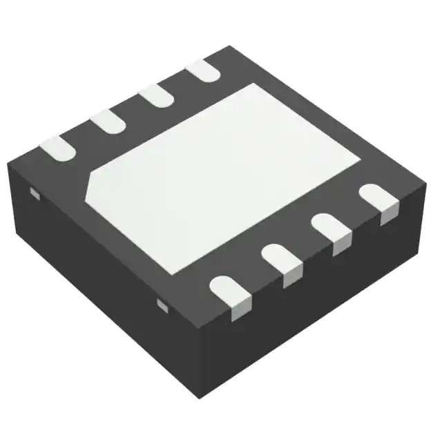
Texas Instruments OPA2314AIDRBR
- Part No.:
- OPA2314AIDRBR
- Manufacturer:
- Texas Instruments
- Category:
- Instrumentation, Op Amps, Buffer Amps
- Package:
- 8-VDFN Exposed Pad
- Datasheet:
-
 OPA2314AIDRBR.pdf
- Description:
- IC CMOS 2 CIRCUIT 8SON
- Quantity:
- Payment:

- Shipping:

Inventory:5,850
Please send an inquiry. Send us your inquiry, and we will respond immediately.
Product details
Overview
OPA2314AIDRBR from Texas Instruments is a dual-channel, rail-to-rail input/output CMOS operational amplifier optimized for low-voltage, low-power applications. It delivers 3 MHz gain-bandwidth, 1.5 V/µs slew rate, 14 nV/√Hz input voltage noise at 1 kHz, 150 µA per channel quiescent current, and 0.5 mV typical input offset voltage - enabling precision signal conditioning in battery-powered instrumentation and portable medical devices.
For engineers reviewing the OPA2314AIDRBR datasheet, OPA2314AIDRBR pinout, OPA2314AIDRBR application, or OPA2314AIDRBR equivalent, key selection considerations include its 1.8–5.5 V supply range, –40°C to 125°C extended temperature rating, integrated RF/EMI filter, unity-gain stability with up to 300 pF capacitive load, and absence of phase reversal under overdrive.
Technical Context
The OPA2314AIDRBR employs a complementary differential input stage enabling rail-to-rail common-mode input range (extending 200 mV beyond both rails), paired with a Class AB output stage capable of driving ≥10 kΩ loads across the full supply range. Its internal architecture includes integrated EMI rejection filtering and robust electrostatic discharge protection (±4 kV HBM).
It achieves unity-gain stability without external compensation while maintaining 65° phase margin at 5 V supply and 10 kΩ load. The device operates with no phase reversal during input overdrive and supports single-supply configurations down to 1.8 V (±0.9 V), making it suitable for direct interfacing with SAR and delta-sigma ADCs requiring wide dynamic range.
Key Specifications
| Parameter | Value and Actual Design Meaning |
|---|---|
| Gain Bandwidth | 3 MHz - enables stable closed-loop operation up to ~200 kHz at G = 10, supporting anti-aliasing and sensor signal conditioning. |
| Slew Rate | 1.5 V/µs - supports clean 100-kHz, 1-Vpp sine wave reproduction without distortion in low-noise front ends. |
| Input Voltage Noise | 14 nV/√Hz at 1 kHz - critical for preserving SNR in photodiode amplifiers and high-impedance sensor interfaces. |
| Quiescent Current | 150 µA per channel - allows dual-amplifier operation on coin-cell or Li-ion sources for >1-year battery life in handheld meters. |
| Input Offset Voltage | 0.5 mV (typical) - ensures ≤0.01% gain error in 5-V full-scale active filters and remote sensing circuits. |
| Supply Range | 1.8 V to 5.5 V - compatible with modern MCU I/O domains and eliminates need for level-shifting in mixed-voltage systems. |
| EMI Rejection | ≥80 dB at 900 MHz - suppresses cellular and ISM-band interference in wireless metering and portable test equipment. |
Pinout & Package
OPA2314AIDRBR is housed in an 8-pin DFN (DRB) package measuring 3.0 mm × 3.0 mm with exposed thermal pad on underside, requiring connection to V– for optimal thermal performance.
| Pin/Terminal | Circuit Role | Design Meaning |
|---|---|---|
| +IN A | Noninverting input, Channel A | Accepts signals from 200 mV below V– to 200 mV above V+; enables true single-supply sensor biasing. |
| –IN A | Inverting input, Channel A | High-impedance node (0.2 pA bias current) - preserves accuracy in MΩ-source transducer interfaces. |
| OUT A | Output, Channel A | Rail-to-rail swing (≤20 mV from rails at 10 kΩ load) - maximizes ADC input dynamic range. |
| V– | Negative supply / ground reference | Must connect exposed thermal pad; serves as return path for both channels and thermal dissipation node. |
| +IN B | Noninverting input, Channel B | Independent input for dual-path signal processing (e.g., differential pair or reference buffer). |
| –IN B | Inverting input, Channel B | Electrically isolated from Channel A inputs - supports independent gain/offset calibration paths. |
| OUT B | Output, Channel B | Capable of simultaneous 3-MHz small-signal response with Channel A - suitable for stereo audio or dual ADC drivers. |
| V+ | Positive supply | Accepts 1.8–5.5 V; requires local 0.01-µF ceramic bypass capacitor to minimize PSRR degradation. |
Key Features
| Feature | Design Value |
|---|---|
| Rail-to-rail input and output | Enables full-supply utilization in 1.8-V systems - extends effective input range by >1.4 V vs conventional op amps. |
| Integrated RF/EMI filter | Rejects GSM/Bluetooth interference without external LC networks - reduces PCB area and layout sensitivity. |
| No phase reversal on overdrive | Prevents latch-up or erroneous control signals when inputs exceed rails - critical for fault-tolerant industrial sensors. |
| Unity-gain stable with 300 pF load | Eliminates need for isolation resistors in capacitive DAC or ADC driver applications - simplifies layout and improves THD. |
| Extended temperature range | Specified from –40°C to +125°C - qualified for under-hood automotive modules and industrial motor control feedback loops. |
Applications
| Battery-Powered Instruments | Photodiode Amplifiers |
|---|---|
Use Scenario: Portable blood glucose meters and handheld multimeters operating from single AA or coin-cell batteries. IC Role / Device Role / Timing Role: Precision transimpedance amplifier and reference buffer for analog front-end signal chain. Use Value: 150 µA/channel quiescent current extends battery life; 0.5 mV offset minimizes calibration drift across temperature. |
Use Scenario: Low-light optical sensing in smoke detectors and environmental particulate monitors. IC Role / Device Role / Timing Role: High-gain, low-noise transimpedance amplifier with DC-coupled output. Use Value: 14 nV/√Hz input noise preserves weak photocurrent SNR; rail-to-rail output drives 12-bit ADC directly. |
| Active Filters | Wireless Metering |
Use Scenario: Anti-aliasing and reconstruction filters in smart utility meters and IoT edge nodes. IC Role / Device Role / Timing Role: Dual-channel second-order Sallen-Key or multiple-feedback topology implementation. Use Value: 3 MHz GBW supports 200-kHz cutoff frequencies; matched dual channels ensure consistent phase response. |
Use Scenario: Sub-GHz RF module sensor interface in AMI (Advanced Metering Infrastructure) endpoints. IC Role / Device Role / Timing Role: Signal conditioning for current/voltage sensing prior to RF SoC ADC sampling. Use Value: Integrated EMI filter rejects 868/915-MHz band noise; 125°C rating supports outdoor enclosure deployment. |
Equivalent & Alternatives
The following parts are listed as comparable options for similar dual-channel, low-power, rail-to-rail op amp applications.
| Alternative Part | Technical Difference | Application Difference | Selection Advice |
|---|---|---|---|
| MCP6022-I/SN | Higher 10 µA IQ, lower 10 kHz GBW (10 MHz), no integrated EMI filter, 2.7–5.5 V supply only | Limited to higher-power, narrowband applications; unsuitable for sub-2-V battery operation or noisy RF environments | Select when cost sensitivity outweighs EMI immunity and ultra-low IQ requirements |
| AD8602ARMZ | Lower 0.25 mV max VOS, higher 1.2 mA IQ, 8 MHz GBW, no rail-to-rail input, –40°C to 125°C rated | Better DC precision but incompatible with 1.8-V supplies and high-impedance sensor biasing due to limited input range | Select when microvolt-level offset is mandatory and supply >2.7 V is guaranteed |
Compared with MCP6022-I/SN and AD8602ARMZ, OPA2314AIDRBR uniquely balances ultra-low power (150 µA), wide supply (1.8–5.5 V), integrated EMI rejection, and rail-to-rail input - making it the only option qualified for long-life, low-voltage, RF-dense portable instrumentation.
Availability
OPA2314AIDRBR is available at Aetrix Electronics and suitable for battery-powered instruments, photodiode amplifiers, and wireless metering applications requiring stable component supply, extended temperature support, and production-ready traceability.
Supply support for OPA2314AIDRBR includes scheduled delivery planning, volume procurement assistance, BOM continuity management, traceable sourcing, and lifecycle availability coordination for OEM customers, industrial embedded developers, connected-device designers, and electronics production programs.
Manufacturer
Texas Instruments is a global semiconductor leader delivering analog and embedded processing solutions, with over 50 years of op amp innovation and broad portfolio coverage from precision to high-speed.
The OPAx314 family was designed specifically for cost-sensitive, battery-constrained applications demanding rail-to-rail operation, low noise, and robust EMI immunity - targeting portable medical, industrial sensing, and energy metering markets.
FAQ
What is the maximum capacitive load the OPA2314AIDRBR can drive while remaining unity-gain stable?
The OPA2314AIDRBR is unity-gain stable with capacitive loads up to 300 pF, as confirmed in the TI SBOS563G datasheet Figure 20 and Section 7.1. This allows direct connection to ADC input capacitors and ceramic bypass networks without series isolation resistors - preserving bandwidth and minimizing THD+N in OPA2314AIDRBR-based data acquisition circuits.
Does the OPA2314AIDRBR support true rail-to-rail input operation below 2.0 V supply?
Yes - the OPA2314AIDRBR maintains rail-to-rail input common-mode range (extending 200 mV beyond both rails) down to 1.8 V supply, verified in Electrical Characteristics Table 6.7 and Figure 7 of SBOS563G. This enables accurate zero-input referencing in 1.8-V MCU systems, unlike many competing op amps that degrade input range below 2.7 V.
How does the integrated RF/EMI filter in the OPA2314AIDRBR improve system-level immunity?
The OPA2314AIDRBR's internal RF/EMI filter provides ≥80 dB rejection at 900 MHz (Figure 32, SBOS563G), suppressing interference from cellular, Bluetooth, and ISM-band transceivers. This eliminates need for external ferrite beads or RC filters in OPA2314AIDRBR signal paths - reducing BOM count and layout sensitivity in wireless metering and portable test equipment.
What is the thermal resistance (RθJA) of the OPA2314AIDRBR in its DRB package?
The OPA2314AIDRBR in the 8-pin DFN (DRB) package has a junction-to-ambient thermal resistance (RθJA) of 53.8°C/W, per Section 6.5 of SBOS563G. This low value - enabled by the exposed thermal pad tied to V– - supports continuous operation at full spec under 125°C ambient conditions when mounted on 2-layer PCBs with adequate copper pour.
Is the OPA2314AIDRBR pin-compatible with other members of the OPAx314 family?
No - the OPA2314AIDRBR (DRB, 8-pin DFN) uses a different pinout than the SOIC-8 (D) and MSOP-8 (DGK) variants of the same device. Pin mapping is identical across packages *within the dual-channel variant*, but mechanical footprint and thermal pad requirements differ. Always verify land pattern against the specific OPA2314AIDRBR DRB mechanical drawing (SLYZ031).
OPA2314AIDRBR Specifications
- Product attributes
- Attribute value
- Manufacturer:
- Texas Instruments
- Series:
- -
- Package/Case:
- 8-VDFN Exposed Pad
- Packaging:
- Tape & Reel (TR)
- Product Status:
- Active
- Amplifier Type:
- CMOS
- Number of Circuits:
- 2
- Output Type:
- Rail-to-Rail
- Slew Rate:
- 1.5V/µs
- Gain Bandwidth Product:
- 3 MHz
- -3db Bandwidth:
- -
- Current - Input Bias:
- 0.2 pA
- Voltage - Input Offset:
- 500 µV
- Current - Supply:
- 150µA (x2 Channels)
- Current - Output / Channel:
- 20 mA
- Voltage - Supply Span (Min):
- 1.8 V
- Voltage - Supply Span (Max):
- 5.5 V
- Operating Temperature:
- -40°C ~ 125°C
- Grade:
- -
- Qualification:
- -
- Mounting Type:
- Surface Mount
- Supplier Device Package:
- 8-SON (3x3)
OPA2314AIDRBR FAQ
1.How can I place an order for OPA2314AIDRBR through Aetrix?
Please submit a Request for Quotation (RFQ) for OPA2314AIDRBR on Aetrix. Our sales agent will provide a competitive quotation and guide you through the order confirmation once you accept the terms.
2.Are the price and stock information for OPA2314AIDRBR reliable?
The price and inventory of OPA2314AIDRBR are updated periodically and may fluctuate due to market conditions. Stock and pricing data are typically refreshed every 24 hours. Quotation validity for OPA2314AIDRBR is usually 5 days.
3.What payment methods are accepted for OPA2314AIDRBR?
We accept Wire Transfer, PayPal, Credit Card, Western Union, MoneyGram, and Escrow for OPA2314AIDRBR transactions.
Note: Certain payment methods may incur a processing fee.
4.How is shipping managed for OPA2314AIDRBR?
OPA2314AIDRBR orders can be shipped via leading logistics carriers, including DHL, UPS, FedEx, TNT, or Registered Mail.
Once your OPA2314AIDRBR order is processed, you will receive an email with the shipment details and tracking number.
Note: Tracking information may take up to 24 hours to appear. Express delivery typically takes 3–5 business days.
5.How can I obtain technical support or documentation for OPA2314AIDRBR?
For technical support, including OPA2314AIDRBR datasheets, pinout diagrams, or application guidance, please contact our engineering support team. They can provide detailed documentation and assistance for your OPA2314AIDRBR requirements.
6.How does Aetrix verify that OPA2314AIDRBR is sourced from the original manufacturer or authorized distributors?
All OPA2314AIDRBR products on Aetrix are procured from qualified distributors and authorized channels. Our dedicated quality assurance team conducts strict verification, including traceability checks and, if necessary, third-party testing. This ensures that OPA2314AIDRBR meets industry standards.
7.What is the process for return or replacement of OPA2314AIDRBR?
All OPA2314AIDRBR units undergo pre-shipment inspection (PSI). If there is an issue with OPA2314AIDRBR, returns or replacements are accepted under the following conditions:
1.Quantity discrepancies, incorrect items, or visible external defects (such as breakage or corrosion), acknowledged by Aetrix.
2.The issue is reported within 90 days of delivery.
3.The OPA2314AIDRBR part is unused and in its original packaging.
Return procedure for OPA2314AIDRBR:
1.Submit a request within 90 days.
2.Obtain a Return Material Authorization (RMA) from Aetrix.
OPA2314AIDRBR Tags

-
LM358DT
STMicroelectronics

-
LM358DR
Texas Instruments
-
LM2904DR
Texas Instruments
-
LM358ADR
Texas Instruments

-
LM2904DGKR
Texas Instruments

-
LM324DR
Texas Instruments

-
MCP6006T-E/OT
Microchip Technology
-
MCP6006UT-E/OT
Microchip Technology

-
LM324PWR
Texas Instruments
-
LM2902PWR
Texas Instruments
-
LM2902DR
Texas Instruments

-
LM358P
Texas Instruments
Tech Hub

A practical engineering guide to 3.3V and 5V logic compatibility, input thresholds, resistor dividers, translator ICs, MOSFET level shifting, I2C pull-ups, timing limits and power-sequencing risks.

The 74HC595 uses push-pull logic outputs, while the TPIC6B595 uses 50 V open-drain DMOS sinks for higher-power loads. This guide compares timing, current limits, 3.3 V interfacing, load wiring, thermal…

The 74HC595 converts serial data into eight stable parallel outputs. This guide covers pin functions, shift and storage timing, OE and MR behavior, drive-current limits, cascading, voltage compatibilit…

A technical comparison of level-sensitive latches and edge-triggered flip-flops, covering timing windows, setup and hold limits, master–slave operation, time borrowing, race-through, HDL inference and…

A D latch stores one bit while Enable controls when data can pass. This reference covers gate-level operation, truth tables, transparency, setup and hold timing, LE versus OE, common ICs and practical …

An SR latch stores one bit through cross-coupled feedback. This engineering reference covers NOR and NAND implementations, truth tables, forbidden-state recovery, gated operation, switch debouncing, fa…

Latch circuits retain one bit through feedback. This technical reference covers SR and D latches, truth tables, transparency, timing limits, latch-versus-flip-flop behavior, applications and common log…

An engineering guide to LED driver operation, constant-current and constant-voltage outputs, linear and switching topologies, dimming, IC selection, calculations, replacement compatibility, and fault c…

Operational amplifier guide covering op amp basics, feedback, ideal vs real op amps, common configurations, buffer circuits, offset, bias current, gain-bandwidth, slew rate, rail-to-rail limits and sel…

Jumper cables guide covering safe connection order, red and black clamp placement, final ground connection, cable gauge, length, clamp quality, copper vs CCA cables, jump starter comparison and battery…


