
 My Inquiry
 My Account


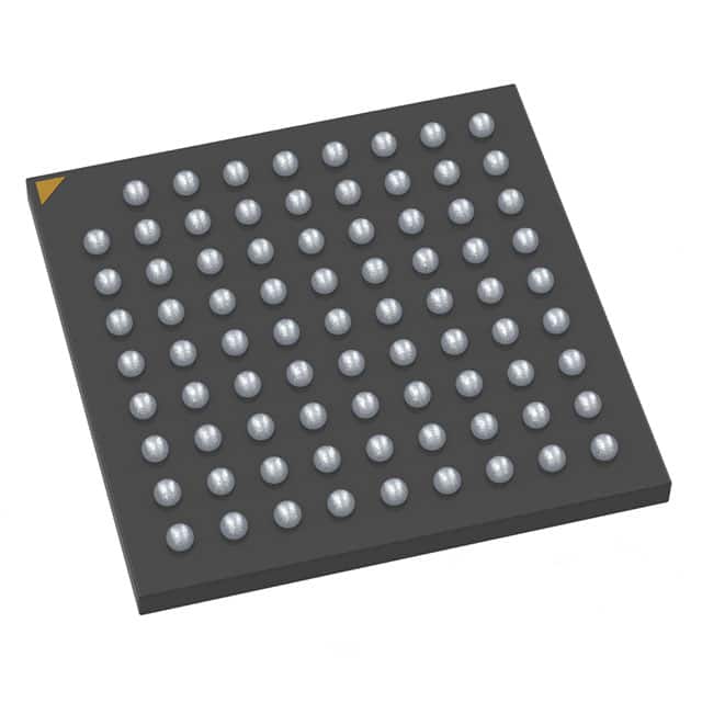
Texas Instruments OPT8320NBP
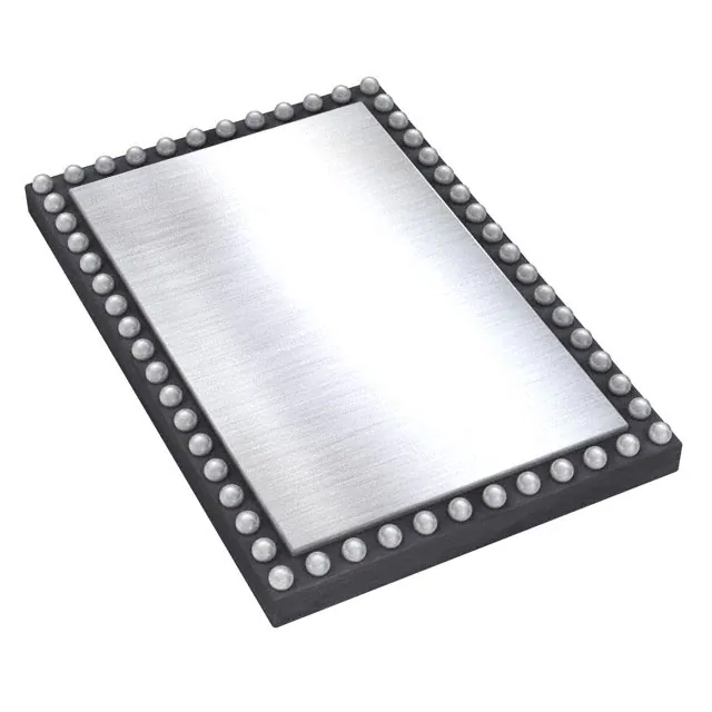
- Part No.:
- OPT8320NBP
- Manufacturer:
- Texas Instruments
- Category:
- Image Sensors, Camera
- Package:
- 56-VFBGA
- Datasheet:
-
 OPT8320NBP.pdf
- Description:
- IC IMAGE SENSOR TOF 3D 56COG
- Quantity:
- Payment:

- Shipping:

Inventory:300
Please send an inquiry. Send us your inquiry, and we will respond immediately.
Product details
Overview
OPT8320NBP from Texas Instruments is a 3D time-of-flight (ToF) sensor system-on-chip (SoC) for depth sensing, featuring an 80 × 60 pixel array, 30 µm pixel pitch, scalable frame rate up to 1000 FPS depth output, integrated illumination driver, and on-chip depth engine computing phase, amplitude, and ambient per pixel. It is used in industrial machine vision systems requiring real-time spatial mapping under varying ambient light.
For engineers reviewing the OPT8320NBP datasheet, OPT8320NBP pinout, OPT8320NBP application, or OPT8320NBP equivalent, key selection considerations include its COG-56 package with optical band-pass filter (830–867 nm), dual-output interface (DVP/SSI), programmable timing generator for motion robustness and SNR optimization, and built-in histogram and calibration support for production-grade depth accuracy.
Technical Context
The OPT8320NBP integrates a timing generator (TG) supporting master/slave sync modes, de-aliasing, high dynamic range via alternate-frame integration scaling, and configurable quad/sub-frame sequencing. Its depth engine computes full-array phase data plus auxiliary amplitude, ambient, and flag outputs - all derived from digitized sensor data without external processing.
It uses a dedicated 24-MHz system clock input (MCLK), supports modulation frequencies from 10 MHz to 100 MHz, and delivers raw ToF data via an 8-lane DVP interface (HD/VD synchronized) or 1-lane SSI. The integrated illumination driver provides up to 150 mA at up to 100 MHz, with PWM control (ILLUM_PWM_CTRL/ILLUM_PWM_SYNC) and feedback (ILLUM_FB) for closed-loop power management.
Key Specifications
| Parameter | Value and Actual Design Meaning |
|---|---|
| Imaging Array | 80 × 60 pixels, 30 µm pitch, 1/6″ format - enables compact, high-resolution depth capture with minimal optical footprint. |
| Depth Output Rate | Scalable up to 1000 FPS - supports high-speed motion capture and real-time gesture response in embedded systems. |
| Demodulation Contrast | 70% at 50 MHz - ensures reliable phase measurement under challenging ambient conditions and low-light scenarios. |
| Illumination Driver | 150 mA max current, 100 MHz max frequency - drives VCSELs or LEDs directly without external drivers, reducing BOM count. |
| Optical Filter | Integrated 830–867 nm band-pass filter - rejects ambient IR noise while maximizing signal-to-noise ratio for 850-nm illumination. |
| Operating Temperature | 0°C to 70°C - qualified for industrial indoor environments including factory automation and kiosk-based AR interfaces. |
| Power Supplies | Separate 1.8-V analog/digital domains + 3.3-V I/O/pixel supplies - enables low-noise analog performance and flexible host interface voltage levels. |
Pinout & Package
OPT8320NBP is housed in a 56-pin Chip-on-Glass (COG) package measuring 8.03 mm × 5.32 mm × 0.745 mm, with integrated optical band-pass filter and fiducials for precise alignment. The exposed thermal pad is non-soldered and must remain electrically isolated.
| Pin/Terminal | Circuit Role | Design Meaning |
|---|---|---|
| MCLK | System clock input | 24-MHz reference required for all internal timing; determines base frame rate and modulation synchronization. |
| OP_DATA[0:7] | Parallel CMOS data output | 8-bit depth/amplitude/ambient data bus; active during HD/VD window - enables high-throughput DVP interface to FPGA or SoC. |
| HD / VD | Horizontal/vertical sync outputs | Indicate active row and frame boundaries - essential for precise image capture timing and ROI alignment in host processors. |
| ILLUM_EN / ILLUM_N / ILLUM_P | Illumination control and modulation | Enable and differential modulation signals for driving external VCSEL arrays - supports high-frequency pulsed illumination with low EMI. |
| I2C_SLV_SCL / I2C_SLV_SDA | Slave configuration interface | Allows register-level programming of timing, ROI, integration duty cycle, and depth engine parameters by host microcontroller. |
| AVDD / DVDD / IOVDD | Supply domain pins | Three independent supply rails (1.8 V analog/digital, 1.8/3.3 V I/O) - prevent noise coupling between sensitive analog pixel circuitry and digital logic. |
Key Features
| Feature | Design Value |
|---|---|
| Programmable Timing Generator | Enables optimization of motion robustness, SNR, and ambient cancellation via configurable quad/sub-frame sequencing and integration duty cycle (13–63 scale). |
| On-Chip Depth Engine | Computes per-pixel phase, amplitude, ambient, and flags - eliminates need for external FPGA/ASIC depth computation, reducing latency and system complexity. |
| High Dynamic Range Mode | Alternate-frame integration scaling (SUP_FRM_INTG_SCALE) allows combined base/supplementary frames to extend usable depth range in mixed-light scenes. |
| Dual Output Interface | Supports both parallel DVP (8-lane, HD/VD sync) and serial SSI (1-lane, clock/chip-select) - simplifies integration into resource-constrained or high-bandwidth host platforms. |
| Integrated Illumination Power Control | Includes PWM sync (ILLUM_PWM_SYNC), feedback (ILLUM_FB), and enable (ILLUM_EN) - enables closed-loop brightness regulation without external analog circuitry. |
Applications
| Industrial Machine Vision | Gesture-Controlled Kiosks |
|---|---|
|
Use Scenario: Real-time bin-picking and part localization in robotic assembly cells with variable lighting and reflective surfaces. IC Role / Device Role / Timing Role: OPT8320NBP acts as the primary depth acquisition node, providing calibrated 80×60 depth maps at ≥60 FPS with ambient rejection enabled via programmable integration timing. Use Value: Built-in histogram and per-pixel ambient data allow adaptive thresholding and background subtraction - improving object segmentation reliability without host CPU overhead. |
Use Scenario: Touchless navigation in public information terminals under fluorescent and daylight illumination. IC Role / Device Role / Timing Role: OPT8320NBP serves as the proximity and gesture sensor, using its 1000-FPS scalable output and de-aliasing frame structure to resolve fast hand motions. Use Value: Integrated illumination driver and optical filter eliminate external IR emitters and lenses - enabling slim, sealed front-panel designs compliant with IP54 ingress protection. |
| 3D Scanning for Quality Inspection | Augmented Reality Alignment |
|
Use Scenario: In-line PCB or molded plastic inspection where sub-millimeter depth resolution is required across curved surfaces. IC Role / Device Role / Timing Role: OPT8320NBP functions as the structured-light alternative, delivering calibrated depth frames with on-chip pixel binning and region-of-interest readout to boost effective SNR. Use Value: Pixel binning (2×2 or 4×4) and ROI configuration reduce data volume while preserving depth fidelity - easing bandwidth constraints on USB or MIPI host interfaces. |
Use Scenario: Spatial anchoring of virtual objects in handheld AR devices using real-world surface geometry. IC Role / Device Role / Timing Role: OPT8320NBP operates as the low-latency depth mapper, feeding phase-aligned depth + amplitude streams to the AR processor's SLAM pipeline. Use Value: Synchronous Serial Interface (SSI) mode provides deterministic timing and reduced pin count - critical for coexistence with camera, IMU, and audio subsystems in portable form factors. |
Equivalent & Alternatives
The following parts are listed as comparable options for similar 3D ToF sensor applications.
| Alternative Part | Technical Difference | Application Difference | Selection Advice |
|---|---|---|---|
| TI OPT8241 | Lower resolution (320×240), higher power consumption, no integrated illumination driver - requires external VCSEL driver and optics. | Targeted at high-accuracy metrology rather than embedded edge sensing; lacks COG packaging and optical filter integration. | Choose OPT8241 only when >300k-pixel resolution and sub-100-µm depth precision are mandatory, and board space/power budget permit external illumination circuitry. |
| Infineon IRS2877C | Single-chip ToF sensor with 224×172 resolution, fixed 30-FPS output, no programmable timing generator or de-aliasing capability. | Designed for automotive cabin monitoring; lacks industrial temperature range and I2C slave configurability for custom timing profiles. | Consider IRS2877C only for cost-sensitive consumer applications where fixed-frame-rate operation and simplified firmware are prioritized over motion robustness or ambient adaptability. |
Compared with OPT8320NBP, OPT8241 offers higher resolution but demands more board area and external components, while IRS2877C reduces design complexity at the expense of configurability and environmental ruggedness - making OPT8320NBP the optimal balance for industrial and interactive embedded depth sensing.
Availability
OPT8320NBP is available at Aetrix Electronics and suitable for industrial machine vision, gesture-controlled kiosks, and 3D scanning applications requiring stable component supply, long-term manufacturability, and consistent optical calibration across production batches.
Supply support for OPT8320NBP includes scheduled delivery planning, volume procurement assistance, BOM continuity management, traceable sourcing, and lifecycle availability coordination for OEM customers, industrial embedded developers, connected-device designers, and electronics production programs.
Manufacturer
Texas Instruments is a global semiconductor company specializing in analog, embedded processing, and sensing technologies, with leadership in industrial, automotive, and communications markets.
The OPT8320NBP belongs to TI's 3D ToF image sensor family, designed specifically for compact, low-power, high-robustness depth sensing in embedded systems where optical integration, ambient immunity, and real-time processing efficiency are critical.
FAQ
What is the maximum frame rate supported by the OPT8320NBP for depth output?
The OPT8320NBP supports a scalable depth output rate up to 1000 FPS, achieved through internal raw frame capture at 4000 FPS and on-chip depth engine processing. This maximum rate assumes full 80×60 array readout, minimal integration time, and DVP interface operation at rated timing margins. Actual sustained frame rate depends on host interface bandwidth and configured ROI size.
Does the OPT8320NBP require an external illumination source?
No, the OPT8320NBP includes a built-in illumination driver capable of delivering up to 150 mA at frequencies up to 100 MHz, sufficient to drive common VCSEL arrays directly. It also provides ILLUM_EN, ILLUM_N/P, ILLUM_PWM_CTRL, and ILLUM_FB pins for precise control and closed-loop regulation - eliminating the need for external driver ICs in most implementations.
How does the OPT8320NBP handle ambient light interference?
The OPT8320NBP combats ambient light via three integrated mechanisms: (1) an on-glass 830–867 nm optical band-pass filter rejecting out-of-band IR; (2) programmable integration timing and de-aliasing frame structures to suppress motion artifacts and harmonic noise; and (3) per-pixel ambient measurement used by the depth engine for real-time background subtraction - all implemented without host processor involvement.
What interface options does the OPT8320NBP provide for depth data output?
The OPT8320NBP offers two configurable output interfaces: an 8-lane Digital Video Port (DVP) with HD/VD synchronization for high-throughput parallel transfer, and a Synchronous Serial Interface (SSI) with single-data-lane, clock, and chip-select for pin-constrained designs. Both interfaces deliver identical depth, amplitude, and ambient data - with SSI offering deterministic timing and lower EMI at the cost of reduced bandwidth.
Is the OPT8320NBP compatible with standard I2C controllers for configuration?
Yes, the OPT8320NBP implements a standard I2C slave interface (I2C_SLV_SCL/I2C_SLV_SDA) operating at up to 400 kHz, allowing direct connection to any microcontroller or SoC with I2C hardware. Configuration registers control all key parameters including timing generator settings, region-of-interest, integration duty cycle, and depth engine behavior - with no proprietary protocol required.
OPT8320NBP Specifications
- Product attributes
- Attribute value
- Manufacturer:
- Texas Instruments
- Series:
- -
- Package/Case:
- 56-VFBGA
- Packaging:
- Tray
- Product Status:
- Active
- Type:
- 3D Time of Flight
- Pixel Size:
- 30µm x 30µm
- Active Pixel Array:
- 80H x 60V
- Frames per Second:
- 1000.0
- Voltage - Supply:
- 1.7V ~ 3.6V
- Supplier Device Package:
- 56-COG (8.07x5.36)
- Operating Temperature:
- 0°C ~ 70°C
- Grade:
- -
- Qualification:
- -
OPT8320NBP FAQ
1.How can I place an order for OPT8320NBP through Aetrix?
Please submit a Request for Quotation (RFQ) for OPT8320NBP on Aetrix. Our sales agent will provide a competitive quotation and guide you through the order confirmation once you accept the terms.
2.Are the price and stock information for OPT8320NBP reliable?
The price and inventory of OPT8320NBP are updated periodically and may fluctuate due to market conditions. Stock and pricing data are typically refreshed every 24 hours. Quotation validity for OPT8320NBP is usually 5 days.
3.What payment methods are accepted for OPT8320NBP?
We accept Wire Transfer, PayPal, Credit Card, Western Union, MoneyGram, and Escrow for OPT8320NBP transactions.
Note: Certain payment methods may incur a processing fee.
4.How is shipping managed for OPT8320NBP?
OPT8320NBP orders can be shipped via leading logistics carriers, including DHL, UPS, FedEx, TNT, or Registered Mail.
Once your OPT8320NBP order is processed, you will receive an email with the shipment details and tracking number.
Note: Tracking information may take up to 24 hours to appear. Express delivery typically takes 3–5 business days.
5.How can I obtain technical support or documentation for OPT8320NBP?
For technical support, including OPT8320NBP datasheets, pinout diagrams, or application guidance, please contact our engineering support team. They can provide detailed documentation and assistance for your OPT8320NBP requirements.
6.How does Aetrix verify that OPT8320NBP is sourced from the original manufacturer or authorized distributors?
All OPT8320NBP products on Aetrix are procured from qualified distributors and authorized channels. Our dedicated quality assurance team conducts strict verification, including traceability checks and, if necessary, third-party testing. This ensures that OPT8320NBP meets industry standards.
7.What is the process for return or replacement of OPT8320NBP?
All OPT8320NBP units undergo pre-shipment inspection (PSI). If there is an issue with OPT8320NBP, returns or replacements are accepted under the following conditions:
1.Quantity discrepancies, incorrect items, or visible external defects (such as breakage or corrosion), acknowledged by Aetrix.
2.The issue is reported within 90 days of delivery.
3.The OPT8320NBP part is unused and in its original packaging.
Return procedure for OPT8320NBP:
1.Submit a request within 90 days.
2.Obtain a Return Material Authorization (RMA) from Aetrix.
OPT8320NBP Tags

-
MT9M114EBLSTCZ-CR
onsemi
-
EPC611-CSP24-001
ESPROS Photonics AG
-
AR0147ATSC00XUEG5-DRBR
onsemi
-
AR0130CSSM00SPCA0-DRBR
onsemi
-
AR1335CSSC11SMKA0-CP
onsemi
-
AR0521SR2M09SURA0-DP
onsemi
-
AR0135CS2M25SUEA0-DPBR
onsemi
-
AR0522SRSC09SURA0-DP
onsemi
-
AR0134CSSC00SPCA0-DPBR
onsemi
-
AR0134CSSM00SUEA0-DPBR
onsemi
-
AR0521SR2C09SURA0-DP
onsemi
-
AR0135CS2M00SUEA0-DPBR
onsemi
Tech Hub

A practical engineering guide to 3.3V and 5V logic compatibility, input thresholds, resistor dividers, translator ICs, MOSFET level shifting, I2C pull-ups, timing limits and power-sequencing risks.

The 74HC595 uses push-pull logic outputs, while the TPIC6B595 uses 50 V open-drain DMOS sinks for higher-power loads. This guide compares timing, current limits, 3.3 V interfacing, load wiring, thermal…

The 74HC595 converts serial data into eight stable parallel outputs. This guide covers pin functions, shift and storage timing, OE and MR behavior, drive-current limits, cascading, voltage compatibilit…

A technical comparison of level-sensitive latches and edge-triggered flip-flops, covering timing windows, setup and hold limits, master–slave operation, time borrowing, race-through, HDL inference and…

A D latch stores one bit while Enable controls when data can pass. This reference covers gate-level operation, truth tables, transparency, setup and hold timing, LE versus OE, common ICs and practical …

An SR latch stores one bit through cross-coupled feedback. This engineering reference covers NOR and NAND implementations, truth tables, forbidden-state recovery, gated operation, switch debouncing, fa…

Latch circuits retain one bit through feedback. This technical reference covers SR and D latches, truth tables, transparency, timing limits, latch-versus-flip-flop behavior, applications and common log…

An engineering guide to LED driver operation, constant-current and constant-voltage outputs, linear and switching topologies, dimming, IC selection, calculations, replacement compatibility, and fault c…

Operational amplifier guide covering op amp basics, feedback, ideal vs real op amps, common configurations, buffer circuits, offset, bias current, gain-bandwidth, slew rate, rail-to-rail limits and sel…

Jumper cables guide covering safe connection order, red and black clamp placement, final ground connection, cable gauge, length, clamp quality, copper vs CCA cables, jump starter comparison and battery…


