
 My Inquiry
 My Account


NXP Semiconductors P2010NXN2KHC
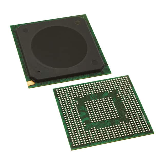
- Part No.:
- P2010NXN2KHC
- Manufacturer:
- NXP Semiconductors
- Category:
- Microprocessors
- Package:
- 689-BBGA Exposed Pad
- Datasheet:
-
 P2010NXN2KHC.pdf
- Description:
- IC MPU QORIQ P2 1GHZ PBGA689
- Quantity:
- Payment:

- Shipping:

Inventory:2,032
Please send an inquiry. Send us your inquiry, and we will respond immediately.
Product details
Overview
P2010NXN2KHC from onsemi is a low-frequency spread spectrum clock generator IC designed to reduce electromagnetic interference at the clock source in embedded and PC peripheral systems. It modulates a single PLL output with up to ±2.5% frequency deviation, supports 10–35 MHz input frequencies, delivers TTL/CMOS-compatible outputs, and operates from 2.7 V to 5.5 V. It is used in printers, scanners, MFPs, and GPS devices to meet FCC EMI requirements without added shielding.
For engineers reviewing the P2010NXN2KHC datasheet, P2010NXN2KHC pinout, P2010NXN2KHC application, or P2010NXN2KHC equivalent, key selection considerations include its selectable spread ranges (±1.25% to ±2.5%), SSON-controlled enable/disable, internal loop filter, 8-pin SOIC/TSSOP packaging, and 360 ps cycle-to-cycle jitter performance.
Technical Context
The P2010NXN2KHC implements an all-digital spread spectrum modulation architecture that sweeps the output clock bandwidth around a center frequency derived from XIN/CLK, reducing peak harmonic amplitudes by up to 20 dB. Its PLL-based synthesis includes integrated feedback and frequency dividers, with modulation rate fixed at (Fin/10) × 20.83 kHz.
It features four digitally selectable spread ranges via FS0 and SR0 pins, internal pull-up/pull-down resistors on control inputs, and a dedicated ModOUT pin delivering the spread clock. The device requires no external loop filter components and supports both crystal and external clock inputs on the XIN/CLK pin.
Key Specifications
| Parameter | Value and Actual Design Meaning |
|---|---|
| Input Frequency Range | 10 MHz to 35 MHz - supports common system clocks for printers, scanners, and embedded controllers without external prescaling. |
| Spread Range Options | ±1.25%, ±1.50%, ±2.00%, ±2.50% - digitally selected via FS0/SR0 to optimize EMI suppression vs. timing margin trade-off. |
| Cycle-to-Cycle Jitter | ≤360 ps - ensures stable timing for synchronous logic interfaces without violating setup/hold margins. |
| Output Drive Strength | 16 mA - sufficient to drive multiple CMOS/TTL loads or trace capacitance up to 15 pF without buffering. |
| Supply Voltage Range | 2.7 V to 5.5 V - enables direct integration into 3.3 V or 5 V legacy and mixed-voltage systems. |
| EMI Reduction | Up to 20 dB - measured peak amplitude reduction of clock harmonics, enabling compliance with FCC Part 15 Class B. |
| Power-Up Lock Time | 0.18 ms - fast PLL lock enables immediate clock availability after power-on, critical for boot-critical peripherals. |
Pinout & Package
Package: 8-pin SOIC (Case 751BD) or TSSOP (Case 948AL), Pb-free and RoHS-compliant. Both packages share identical pin numbering and function mapping.
| Pin/Terminal | Circuit Role | Design Meaning |
|---|---|---|
| XIN / CLK | Input | Accepts either crystal oscillator connection or externally generated clock signal - dual-mode interface reduces BOM count. |
| XOUT | Input (crystal mode only) | Connects to crystal's output terminal; left unconnected when using external clock - eliminates need for mode-select jumpers. |
| FS0 | Digital Control Input | Selects input frequency band (10–20 MHz or 20–35 MHz); internal pull-up enables default high-state operation. |
| VSS | Ground | Dedicated ground reference for analog and digital sections - separation minimizes noise coupling into PLL core. |
| SSON | Digital Control Input | Active-low enable for spread spectrum; internal pull-low allows default disabled state - supports fail-safe EMI control. |
| ModOUT | Output | Dedicated spread-spectrum clock output; electrically isolated from XIN/XOUT path to prevent feedback contamination. |
| SR0 | Digital Control Input | Selects spread percentage (±1.25% to ±2.50%); internal pull-up simplifies PCB layout with minimal external components. |
| VDD | Power Supply | Single-supply input supporting 3.3 V or 5 V operation - eliminates need for level shifters in mixed-voltage designs. |
Key Features
| Feature | Design Value |
|---|---|
| FCC-approved spread spectrum method | Validated modulation profile meets FCC Part 15 radiated emission limits without board-level shielding. |
| Internal loop filter | Removes requirement for external RC network - saves 2–3 passive components and ≥2 mm² PCB area per unit. |
| Four selectable spread ranges | Enables system-specific EMI tuning: lower spread for timing-sensitive subsystems, higher spread for noise-dominated environments. |
| TTL/CMOS-compatible outputs | Direct interface with standard logic families without translation - avoids added propagation delay or power consumption. |
| Low cycle-to-cycle jitter (≤360 ps) | Maintains timing integrity for synchronous peripherals such as USB PHYs, parallel printer interfaces, and memory controllers. |
Applications
| Printer Engine Timing | Flatbed Scanner Clocking |
|---|---|
|
Use Scenario: High-speed laser printer engine requiring precise motor and laser diode synchronization at 16 MHz. IC Role / Device Role / Timing Role: Spread spectrum clock generator providing EMI-compliant 16 MHz clock to ASIC timing controller and stepper driver. Use Value: Reduces radiated emissions from the 16 MHz fundamental and its harmonics by up to 20 dB, eliminating need for metal shielding over the timing section. |
Use Scenario: Flatbed scanner using CIS sensor array and ADC sampling at 20 MHz. IC Role / Device Role / Timing Role: Generates spread-spectrum clock for image sensor timing and ADC sampling circuitry to suppress narrowband noise peaks. Use Value: Enables Class B EMI compliance without increasing PCB layer count or adding ferrite beads on clock traces. |
| MFP System Clock Management | GPS Module Reference Clock |
|
Use Scenario: Multi-function peripheral integrating print, scan, and fax functions sharing a common 25 MHz system clock. IC Role / Device Role / Timing Role: Centralized spread spectrum clock source feeding multiple subsystems including USB host, JPEG encoder, and memory interface. Use Value: Lowers broadband EMI across entire MFP chassis, allowing single-layer ground plane instead of split-ground isolation between analog/digital sections. |
Use Scenario: Portable GPS receiver requiring low-noise 10 MHz reference clock for RF front-end and baseband processor. IC Role / Device Role / Timing Role: Provides FCC-compliant 10 MHz spread clock to GPS SoC's PLL reference input while maintaining <360 ps jitter. Use Value: Prevents clock-related spurs from degrading GPS sensitivity below −145 dBm without compromising acquisition time. |
Equivalent & Alternatives
The following parts are listed as comparable options for similar spread spectrum clock generation applications.
| Alternative Part | Technical Difference | Application Difference | Selection Advice |
|---|---|---|---|
| ICS9172A-01T | Fixed ±0.5% spread range; no digital select pins; requires external loop filter components. | Limited to low-spread applications where EMI margin is modest; not suitable for high-spread regulatory targets like FCC Class B. | Choose when system clock stability is prioritized over maximum EMI reduction and board space is not constrained. |
| Si5330B-A-GM | Programmable via I²C; supports multi-output, jitter cleaning, and wider input range (up to 710 MHz); higher cost and complexity. | Used in high-performance timing systems requiring jitter attenuation and clock distribution - over-engineered for basic EMI reduction. | Choose only if future scalability to multi-clock domains or sub-ps jitter performance is required; otherwise, P2010NXN2KHC offers optimal cost/performance balance. |
Compared with ICS9172A-01T and Si5330B-A-GM, the P2010NXN2KHC delivers targeted EMI suppression with minimal component count and zero configuration overhead, making it ideal for cost-sensitive, volume-manufactured peripherals where simplicity and FCC compliance are primary design goals.
Availability
P2010NXN2KHC is available at Aetrix Electronics and suitable for printers, scanners, and MFPs requiring stable component supply, FCC-compliant clocking, and long-term industrial temperature support.
Supply support for P2010NXN2KHC includes scheduled delivery planning, volume procurement assistance, BOM continuity management, traceable sourcing, and lifecycle availability coordination for OEM customers, industrial embedded developers, connected-device designers, and electronics production programs.
Manufacturer
onsemi (formerly ON Semiconductor) is a global semiconductor supplier specializing in energy-efficient power, analog, sensing, and connectivity solutions for automotive, industrial, cloud, and consumer markets.
The P2010NXN2KHC belongs to onsemi's low-frequency EMI reduction IC product line, engineered specifically to simplify FCC Class B compliance in cost-sensitive PC peripherals and embedded controllers without sacrificing timing integrity.
FAQ
What is the primary function of the P2010NXN2KHC?
The P2010NXN2KHC is a spread spectrum clock generator IC that reduces electromagnetic interference by modulating the output frequency of a PLL within ±1.25% to ±2.50%. It accepts input clocks from 10 MHz to 35 MHz and delivers a low-jitter, EMI-compliant clock on the ModOUT pin. Its all-digital implementation and internal loop filter make the P2010NXN2KHC ideal for embedded controllers and PC peripherals where board space and shielding cost must be minimized.
Does the P2010NXN2KHC require external components to operate?
No, the P2010NXN2KHC operates with zero external passive components for loop filtering due to its integrated digital loop architecture. Only decoupling capacitors (e.g., 0.1 µF near VDD) are recommended. The XIN/CLK and XOUT pins support either crystal or external clock inputs - no additional mode-selection hardware is needed. This makes the P2010NXN2KHC a drop-in solution for EMI reduction without redesigning the clock path.
How does the SSON pin control spread spectrum operation in the P2010NXN2KHC?
The SSON pin is an active-low digital input that enables or disables spread spectrum modulation. When pulled low, the P2010NXN2KHC applies frequency spreading to the ModOUT signal; when high (or left floating, due to internal pull-down), spreading is disabled and ModOUT mirrors the unmodulated PLL output. This allows runtime EMI control - for example, disabling spread during system diagnostics or calibration sequences where deterministic timing is required.
What package options are available for the P2010NXN2KHC?
The P2010NXN2KHC is offered in two industry-standard packages: 8-pin SOIC (Case 751BD, 150-mil width) and 8-pin TSSOP (Case 948AL, 4.4 mm × 3.0 mm). Both are Pb-free and RoHS-compliant. The pinout and electrical characteristics are identical across packages, enabling footprint interchangeability during prototyping or cost optimization without changing schematic or firmware.
Can the P2010NXN2KHC be used with a 5 V supply?
Yes, the P2010NXN2KHC supports a supply voltage range of 2.7 V to 5.5 V, making it fully compatible with 5 V systems. Its TTL/CMOS-compatible outputs maintain valid logic levels across this range, and its internal regulators ensure consistent modulation depth and jitter performance regardless of VDD. This allows direct integration into legacy 5 V printer or scanner designs without level-shifting circuitry.
P2010NXN2KHC Specifications
- Product attributes
- Attribute value
- Manufacturer:
- NXP Semiconductors
- Package/Case:
- 689-BBGA Exposed Pad
- Series:
- QorIQ P2
- Packaging:
- Bulk
- Product Status:
- Obsolete
- Core Processor:
- PowerPC e500v2
- Number of Cores/Bus Width:
- 1 Core, 32-Bit
- Speed:
- 1GHz
- Co-Processors/DSP:
- -
- RAM Controllers:
- DDR2, DDR3
- Graphics Acceleration:
- No
- Display & Interface Controllers:
- -
- Ethernet:
- 10/100/1000Mbps (3)
- SATA:
- -
- USB:
- USB 2.0 + PHY (2)
- Voltage - I/O:
- 1.5V, 1.8V, 2.5V, 3.3V
- Operating Temperature:
- -40°C ~ 125°C (TJ)
- Grade:
- -
- Qualification:
- -
- Security Features:
- -
- Mounting Type:
- Surface Mount
- Supplier Device Package:
- 689-TEPBGA II (31x31)
- Additional Interfaces:
- DMA, DUART, GPIO, I2C, MMC/SD, PCIe, SPI
P2010NXN2KHC FAQ
1.How can I place an order for P2010NXN2KHC through Aetrix?
Please submit a Request for Quotation (RFQ) for P2010NXN2KHC on Aetrix. Our sales agent will provide a competitive quotation and guide you through the order confirmation once you accept the terms.
2.Are the price and stock information for P2010NXN2KHC reliable?
The price and inventory of P2010NXN2KHC are updated periodically and may fluctuate due to market conditions. Stock and pricing data are typically refreshed every 24 hours. Quotation validity for P2010NXN2KHC is usually 5 days.
3.What payment methods are accepted for P2010NXN2KHC?
We accept Wire Transfer, PayPal, Credit Card, Western Union, MoneyGram, and Escrow for P2010NXN2KHC transactions.
Note: Certain payment methods may incur a processing fee.
4.How is shipping managed for P2010NXN2KHC?
P2010NXN2KHC orders can be shipped via leading logistics carriers, including DHL, UPS, FedEx, TNT, or Registered Mail.
Once your P2010NXN2KHC order is processed, you will receive an email with the shipment details and tracking number.
Note: Tracking information may take up to 24 hours to appear. Express delivery typically takes 3–5 business days.
5.How can I obtain technical support or documentation for P2010NXN2KHC?
For technical support, including P2010NXN2KHC datasheets, pinout diagrams, or application guidance, please contact our engineering support team. They can provide detailed documentation and assistance for your P2010NXN2KHC requirements.
6.How does Aetrix verify that P2010NXN2KHC is sourced from the original manufacturer or authorized distributors?
All P2010NXN2KHC products on Aetrix are procured from qualified distributors and authorized channels. Our dedicated quality assurance team conducts strict verification, including traceability checks and, if necessary, third-party testing. This ensures that P2010NXN2KHC meets industry standards.
7.What is the process for return or replacement of P2010NXN2KHC?
All P2010NXN2KHC units undergo pre-shipment inspection (PSI). If there is an issue with P2010NXN2KHC, returns or replacements are accepted under the following conditions:
1.Quantity discrepancies, incorrect items, or visible external defects (such as breakage or corrosion), acknowledged by Aetrix.
2.The issue is reported within 90 days of delivery.
3.The P2010NXN2KHC part is unused and in its original packaging.
Return procedure for P2010NXN2KHC:
1.Submit a request within 90 days.
2.Obtain a Return Material Authorization (RMA) from Aetrix.
P2010NXN2KHC Tags

-
AT91SAM9260B-CU-999
Microchip Technology
-
AT91SAM9G25-CU
Microchip Technology

-
ATSAMA5D27C-CU
Microchip Technology
-
AT91SAM9X35-CU
Microchip Technology
-
AT91SAM9X25-CU
Microchip Technology

-
MCIMX6Y2CVM08AB
NXP Semiconductors
.JPG)
-
AM3352BZCZ100
Texas Instruments
-
AT91SAM9260B-CU
Microchip Technology

-
AT91SAM9260B-QU
Microchip Technology

-
ATSAMA5D31A-CU
Microchip Technology
-
AT91SAM9G20B-CU-999
Microchip Technology
-
MCIMX6Y2CVM05AB
NXP Semiconductors
Tech Hub

A practical engineering guide to 3.3V and 5V logic compatibility, input thresholds, resistor dividers, translator ICs, MOSFET level shifting, I2C pull-ups, timing limits and power-sequencing risks.

The 74HC595 uses push-pull logic outputs, while the TPIC6B595 uses 50 V open-drain DMOS sinks for higher-power loads. This guide compares timing, current limits, 3.3 V interfacing, load wiring, thermal…

The 74HC595 converts serial data into eight stable parallel outputs. This guide covers pin functions, shift and storage timing, OE and MR behavior, drive-current limits, cascading, voltage compatibilit…

A technical comparison of level-sensitive latches and edge-triggered flip-flops, covering timing windows, setup and hold limits, master–slave operation, time borrowing, race-through, HDL inference and…

A D latch stores one bit while Enable controls when data can pass. This reference covers gate-level operation, truth tables, transparency, setup and hold timing, LE versus OE, common ICs and practical …

An SR latch stores one bit through cross-coupled feedback. This engineering reference covers NOR and NAND implementations, truth tables, forbidden-state recovery, gated operation, switch debouncing, fa…

Latch circuits retain one bit through feedback. This technical reference covers SR and D latches, truth tables, transparency, timing limits, latch-versus-flip-flop behavior, applications and common log…

An engineering guide to LED driver operation, constant-current and constant-voltage outputs, linear and switching topologies, dimming, IC selection, calculations, replacement compatibility, and fault c…

Operational amplifier guide covering op amp basics, feedback, ideal vs real op amps, common configurations, buffer circuits, offset, bias current, gain-bandwidth, slew rate, rail-to-rail limits and sel…

Jumper cables guide covering safe connection order, red and black clamp placement, final ground connection, cable gauge, length, clamp quality, copper vs CCA cables, jump starter comparison and battery…


