
 My Inquiry
 My Account


Diodes Incorporated PAM8904EJER
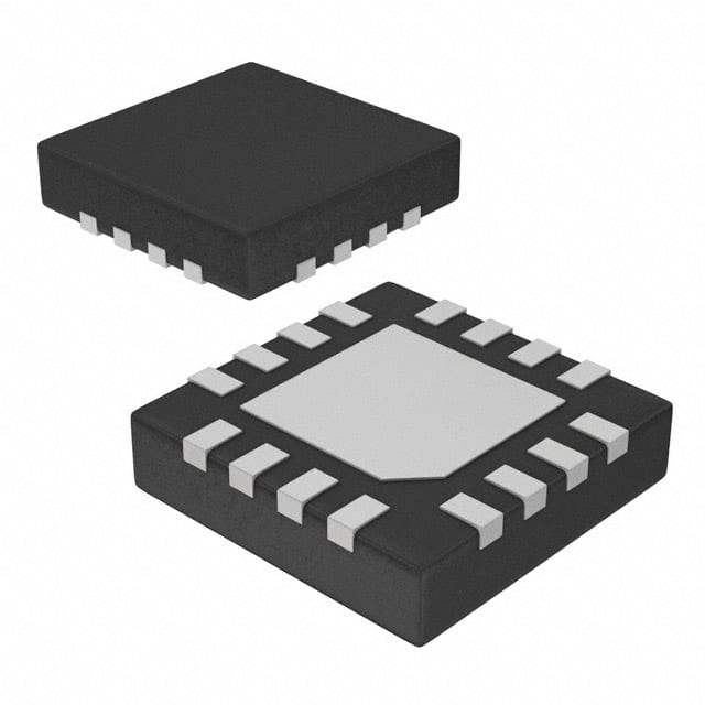
- Part No.:
- PAM8904EJER
- Manufacturer:
- Diodes Incorporated
- Category:
- Specialized ICs
- Package:
- 16-UFQFN Exposed Pad
- Datasheet:
-
 PAM8904EJER.pdf
- Description:
- IC PIEZO SOUNDER DRVR 16UQFN
- Quantity:
- Payment:

- Shipping:

Inventory:4,378
Please send an inquiry. Send us your inquiry, and we will respond immediately.
Product details
Overview
PAM8904EJER from Diodes Incorporated is a piezoelectric sounder driver IC with integrated 3x charge pump boost converter, delivering up to 18VPP output from a 3V supply and supporting differential or single-ended ceramic sounder drive up to 47nF load. It operates across 1.5–5.5V input, features automatic standby/wake-up control, and includes thermal shutdown, overcurrent protection, and undervoltage lockout - deployed in health care alarms and security devices.
For engineers reviewing the PAM8904EJER datasheet, PAM8904EJER pinout, PAM8904EJER application, or PAM8904EJER equivalent, this page delivers verified package mapping (U-QFN3030-16 Type B), confirmed charge pump mode selection logic (EN1/EN2), real-world timing values (tON up to 1.91ms), and validated differential/single-ended output configuration options.
Technical Context
The PAM8904EJER implements a fixed-frequency 100kHz charge pump with selectable 1x/2x/3x multiplication, generating up to 13.5V from 3V input while maintaining low EMI via Diodes' proprietary drive architecture. Its dual-output stage (VO1/VO2) supports both differential and single-ended piezo drive modes with no voltage cross during shutdown.
Control logic interprets EN1/EN2 states to select operating mode or force shutdown, while DIN accepts 20Hz–300kHz rectangular input signals. Internal protection includes short-circuit current limiting (49mA), thermal shutdown at +150°C junction temperature, and undervoltage lockout below 1.5V.
Key Specifications
| Parameter | Value and Actual Design Meaning |
|---|---|
| Supply Voltage Range | 1.5V to 5.5V - Enables direct battery operation from single Li-ion or triple-AA cells without external LDO. |
| Output Voltage (3x Mode) | 7.2–9.0V (VIN=3.0V) - Delivers 18VPP differential swing for high-SPL piezo sounders requiring >12V drive. |
| Charge Pump Frequency | Fixed 100kHz (70–130kHz range) - Optimized for minimal external capacitor size (1µF CP1/CP2) and low EMI radiation. |
| Load Capacitance Support | Up to 47nF - Matches standard ceramic sounder capacitance without external buffering or impedance matching. |
| Startup Delay (3x Mode) | 1.91ms typical - Ensures stable VOUT ramp before VO1/VO2 activation, preventing audible click transients. |
| Shutdown Current | 0.008–1µA - Extends battery life in intermittent alarm applications with long standby intervals. |
| Input Signal Bandwidth | 20Hz to 300kHz - Supports ultrasonic cleaning drivers and multi-tone alarm generation without aliasing. |
Pinout & Package
Package: U-QFN3030-16 (Type B), 3.0mm × 3.0mm × 0.6mm, 16-pin, exposed thermal pad, RoHS-compliant NiPdAu terminations.
| Pin | Circuit Role | Design Meaning |
|---|---|---|
| 1 | NC | No connection - Must be left floating or grounded per layout guidelines; not internally bonded. |
| 2 | VIN | Main power input - Supplies internal logic and charge pump; requires 2.2µF ceramic decoupling adjacent to pin. |
| 3 | CP2 | Charge pump capacitor positive terminal - Connects to C2 (1µF) for 2nd-stage pumping; shared with CP1 in 1x/2x modes. |
| 4 | VOUT | Boosted supply output - Provides regulated 3x VIN to output stage; powers VO1/VO2 drivers directly. |
| 5 | CN1 | Charge pump capacitor negative terminal - Returns C1 (1µF) to ground; forms first-stage flying capacitor node. |
| 6 | GND | Power and signal reference - Shared ground plane required under exposed thermal pad for thermal performance. |
| 7 | VO2 | Positive output driver - Drives one side of differential piezo load; swings rail-to-rail relative to VO1. |
| 8 | NC | No connection - Not bonded; must not be connected to any net to avoid parasitic coupling. |
| 9 | VO1 | Negative output driver - Complementary to VO2; enables true differential drive for maximum sound pressure. |
| 10 | CN2 | Charge pump capacitor negative terminal - Returns C2 (1µF) to ground; completes second-stage flying capacitor path. |
| 11 | CP1 | Charge pump capacitor positive terminal - Connects to C1 (1µF); primary flying node for 1x/2x/3x voltage doubling/tripling. |
| 12 | NC | No connection - Unbonded; PCB pad should be omitted or tied to GND only if required by mechanical design. |
| 13 | VOUT | Boosted supply output - Duplicate VOUT pin (same net as Pin 4); improves current sharing and reduces IR drop. |
| 14 | CP2 | Charge pump capacitor positive terminal - Duplicate CP2 pin (same net as Pin 3); enhances charge transfer efficiency. |
| 15 | VIN | Main power input - Duplicate VIN pin (same net as Pin 2); lowers input impedance and improves PSRR. |
| 16 | NC | No connection - Unbonded; no electrical function; may be used for mechanical anchoring only. |
Key Features
| Feature | Design Value |
|---|---|
| Integrated 3x charge pump | Eliminates need for external boost IC or inductor, reducing BOM count by ≥3 components and PCB area by >25mm². |
| Differential + single-ended output support | Enables same IC to drive either high-efficiency differential piezos (e.g., medical alert buzzers) or cost-sensitive single-ended loads (e.g., smoke detector indicators). |
| Automatic standby/wake-up | Reduces average system current by >99% during idle periods without requiring host MCU intervention or firmware timers. |
| Low EMI drive architecture | Meets CISPR 22 Class B radiated emissions limits without ferrite beads or shielding, simplifying EMC certification. |
| Built-in protection suite | Thermal shutdown, overcurrent limit (49mA), overvoltage clamp (15V), and UVLO prevent field failures in unregulated battery systems. |
Applications
| Medical Alert Systems | Smart Home Security Alarms |
|---|---|
|
Use Scenario: Battery-powered wearable fall-detection pendants emitting audible alerts upon impact detection. IC Role / Device Role / Timing Role: Piezo driver providing 18VPP differential output to generate >85dB SPL at 2.5kHz with <1.91ms startup delay. Use Value: Extended battery life (≤1µA shutdown current) and immunity to voltage sag during alarm bursts due to local 3x boost supply. |
Use Scenario: Wireless door/window sensor modules triggering piercing alarm tones when intrusion is detected. IC Role / Device Role / Timing Role: Single-ended piezo driver activated by GPIO from sub-GHz RF SoC; responds within 470µs (1x mode) to minimize latency. Use Value: Eliminates need for separate boost converter, enabling compact 12mm × 12mm PCB footprint while sustaining 10-year coin-cell operation. |
| Portable Health Monitors | Kitchen Appliance Timers |
|
Use Scenario: Handheld blood glucose meters using tactile piezo feedback for button press confirmation. IC Role / Device Role / Timing Role: Low-power piezo driver operating from 3V coin cell; enters auto-standby after 42ms signal absence. Use Value: Prevents audible "pop" on power-up/down via no-cross shutdown and enables <100nA average current in sleep state. |
Use Scenario: Microwave oven control panels generating distinct tone sequences for timer completion and error conditions. IC Role / Device Role / Timing Role: Dual-mode driver switching between 1x (low-tone) and 3x (high-tone) via EN1/EN2 pins under MCU control. Use Value: One IC replaces two discrete drivers, reducing component count and enabling programmable tone profiles without hardware change. |
Equivalent & Alternatives
The following parts are listed as comparable options for similar piezo sounder driver applications.
| Alternative Part | Technical Difference | Application Difference | Selection Advice |
|---|---|---|---|
| Texas Instruments TPS61175 | Inductor-based boost (not charge pump); requires external MOSFET and diode; 2.5MHz switching; no integrated piezo driver stage. | Needs external H-bridge or amplifier for piezo drive; higher EMI; larger solution size. | Select only when >20V output or >100mA drive current is required beyond PAM8904EJER's 47nF/18VPP capability. |
| Rohm BU9000KV | Fixed 2x charge pump only; no 1x/3x selection; 12VPP max output; no differential drive; no auto-standby. | Limited to single-ended loads; lacks dynamic mode switching and ultra-low shutdown current. | Choose for cost-sensitive, low-feature applications where 12VPP and basic on/off control suffice. |
Compared with TPS61175 and BU9000KV, the PAM8904EJER uniquely integrates mode-selectable charge pump, differential output stage, and autonomous power management - delivering lowest component count, smallest footprint, and longest battery life for piezo-driven audio alerts.
Availability
PAM8904EJER is available at Aetrix Electronics and suitable for medical alert systems, smart home security alarms, portable health monitors, and kitchen appliance timers requiring stable component supply and long-term lifecycle support.
Supply support for PAM8904EJER includes scheduled delivery planning, volume procurement assistance, BOM continuity management, traceable sourcing, and lifecycle availability coordination for OEM customers, industrial embedded developers, connected-device designers, and electronics production programs.
Manufacturer
Diodes Incorporated is a global semiconductor company specializing in discrete, analog, and mixed-signal solutions, with design centers across Asia, Europe, and the US.
The PAM8904E belongs to Diodes' audio interface and power management product line, engineered specifically for ultra-low-power, high-voltage piezo actuation in battery-constrained consumer and healthcare electronics.
FAQ
What is the maximum piezo capacitance the PAM8904EJER can drive reliably?
The PAM8904EJER is characterized and guaranteed to drive loads up to 47nF, as confirmed in Electrical Characteristics (DS41667 Rev. 4–2, page 4). This value corresponds to typical ceramic sounders used in medical and security applications. Driving >47nF may cause extended tON, reduced output amplitude, or thermal stress under continuous operation.
Can the PAM8904EJER operate from a 1.8V supply?
Yes - the PAM8904EJER supports 1.5V to 5.5V input, including 1.8V. At 1.8V, 3x mode yields ~5.4V VOUT, enabling 10.8VPP differential output. However, output voltage scales linearly: 18VPP is only achievable from ≥3V supply, per DS41667 Section 4 (page 1).
How does the automatic shutdown/wake-up function interact with the EN1/EN2 pins?
When DIN is inactive for >42ms, the IC enters auto-standby regardless of EN1/EN2 state. Wake-up occurs on next valid DIN edge. EN1/EN2 retain mode-setting function during wake-up but do not override auto-standby behavior - they only force immediate shutdown when both are low (per Table on page 5).
Is the U-QFN3030-16 (Type B) package thermally enhanced compared to other variants?
Yes - the U-QFN3030-16 (Type B) has θJA = 35°C/W and θJC = 14°C/W (DS41667 Rev. 4–2, page 3), significantly lower than U-QFN2020-12 variants (θJA = 68°C/W). Its larger die pad and dual VIN/VOUT pins improve heat dissipation, making it preferred for continuous-tone applications above 1kHz.
PAM8904EJER Specifications
- Product attributes
- Attribute value
- Manufacturer:
- Diodes Incorporated
- Series:
- -
- Package/Case:
- 16-UFQFN Exposed Pad
- Packaging:
- Tape & Reel (TR)
- Product Status:
- Active
- Programmable:
- Not Verified
- Type:
- Piezo Sounder Driver
- Applications:
- Health, Home, Security
- Mounting Type:
- Surface Mount
- Supplier Device Package:
- U-QFN3030-16 (Type B)
- Grade:
- -
- Qualification:
- -
PAM8904EJER FAQ
1.How can I place an order for PAM8904EJER through Aetrix?
Please submit a Request for Quotation (RFQ) for PAM8904EJER on Aetrix. Our sales agent will provide a competitive quotation and guide you through the order confirmation once you accept the terms.
2.Are the price and stock information for PAM8904EJER reliable?
The price and inventory of PAM8904EJER are updated periodically and may fluctuate due to market conditions. Stock and pricing data are typically refreshed every 24 hours. Quotation validity for PAM8904EJER is usually 5 days.
3.What payment methods are accepted for PAM8904EJER?
We accept Wire Transfer, PayPal, Credit Card, Western Union, MoneyGram, and Escrow for PAM8904EJER transactions.
Note: Certain payment methods may incur a processing fee.
4.How is shipping managed for PAM8904EJER?
PAM8904EJER orders can be shipped via leading logistics carriers, including DHL, UPS, FedEx, TNT, or Registered Mail.
Once your PAM8904EJER order is processed, you will receive an email with the shipment details and tracking number.
Note: Tracking information may take up to 24 hours to appear. Express delivery typically takes 3–5 business days.
5.How can I obtain technical support or documentation for PAM8904EJER?
For technical support, including PAM8904EJER datasheets, pinout diagrams, or application guidance, please contact our engineering support team. They can provide detailed documentation and assistance for your PAM8904EJER requirements.
6.How does Aetrix verify that PAM8904EJER is sourced from the original manufacturer or authorized distributors?
All PAM8904EJER products on Aetrix are procured from qualified distributors and authorized channels. Our dedicated quality assurance team conducts strict verification, including traceability checks and, if necessary, third-party testing. This ensures that PAM8904EJER meets industry standards.
7.What is the process for return or replacement of PAM8904EJER?
All PAM8904EJER units undergo pre-shipment inspection (PSI). If there is an issue with PAM8904EJER, returns or replacements are accepted under the following conditions:
1.Quantity discrepancies, incorrect items, or visible external defects (such as breakage or corrosion), acknowledged by Aetrix.
2.The issue is reported within 90 days of delivery.
3.The PAM8904EJER part is unused and in its original packaging.
Return procedure for PAM8904EJER:
1.Submit a request within 90 days.
2.Obtain a Return Material Authorization (RMA) from Aetrix.
PAM8904EJER Tags

-
CAP200DG-TL
Power Integrations
-
ATSHA204A-MAHDA-T
Microchip Technology

-
ATSHA204A-SSHDA-T
Microchip Technology

-
ATSHA204A-STUCZ-T
Microchip Technology
-
ATECC608B-MAHDA-T
Microchip Technology
-
ATECC608B-MAHCZ-S
Microchip Technology

-
ATECC608B-SSHDA-T
Microchip Technology
-
ATECC608B-MAHDA-S
Microchip Technology
-
ATECC608A-MAHDA-S
Microchip Technology
-
ATECC608B-MAVDA-T
Microchip Technology

-
ATECC608A-SSHDA-T
Microchip Technology
-
ATECC508A-MAHDA-T
Microchip Technology
Tech Hub

Operational amplifier guide covering op amp basics, feedback, ideal vs real op amps, common configurations, buffer circuits, offset, bias current, gain-bandwidth, slew rate, rail-to-rail limits and sel…

Jumper cables guide covering safe connection order, red and black clamp placement, final ground connection, cable gauge, length, clamp quality, copper vs CCA cables, jump starter comparison and battery…

LDO regulator guide covering low dropout voltage, power dissipation, thermal design, PSRR, output noise, capacitor stability, adjustable LDO circuits, LDO vs buck converter and datasheet selection chec…

Conditional Access Module guide covering CAM meaning, CI/CI+ interface, smart card authorization, DVB security workflow, TV and set-top box compatibility, internal electronics, ESD protection, connecto…

Guide to electronic component obsolescence covering EOL risk, PCN/PDN notices, last-time buy planning, replacement options, form-fit-function validation, counterfeit risk and BOM lifecycle management.

18650 battery guide covering lithium-ion cell basics, 3.6V/3.7V voltage, 4.2V charging, mAh and Wh capacity, protected cells, chargers, BMS, series-parallel packs, holders, welding and sourcing checks.…

Hall effect sensor guide covering working principle, linear and digital sensors, Arduino circuits, current sensing, speed detection, automotive applications, A3144 examples, signal filtering and datash…

Product Change Notification guide for electronic components, covering PCN meaning, PCN vs PDN/EOL, common change types, risk levels, form-fit-function review, engineering validation, BOM control, LTB/L…

A practical guide to blend door actuators, covering HVAC function, symptoms, location, AC and heater issues, reset and calibration, replacement cost, electrical diagnosis, compatibility checks, and rep…

Engineering guide to Raspberry Pi alternatives, covering chip-level differences, Orange Pi, ROCK, Jetson, Banana Pi, NanoPi, Compute Module, Pico, GPIO, camera, HAT compatibility, and replacement risks…


