
 My Inquiry
 My Account


NXP Semiconductors PCA9661B,118
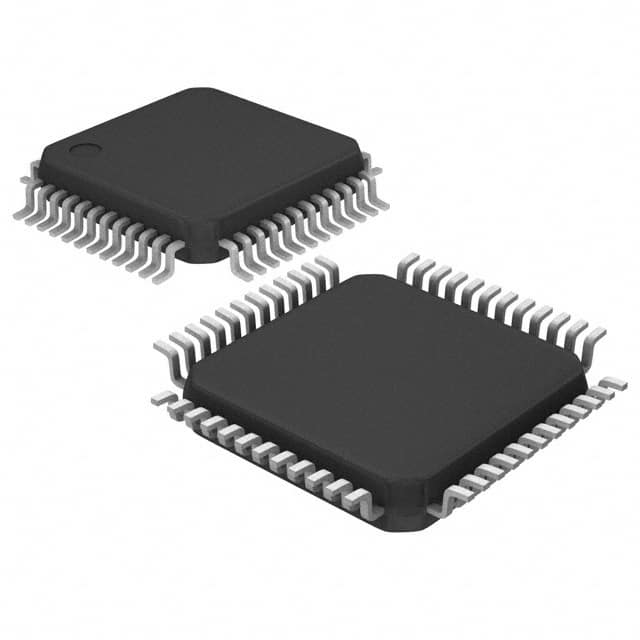
- Part No.:
- PCA9661B,118
- Manufacturer:
- NXP Semiconductors
- Category:
- Controllers
- Package:
- 48-LQFP
- Datasheet:
-
 PCA9661B,118.pdf
- Description:
- IC CTRLR PAR-I2C BUS 48LQFP
- Quantity:
- Payment:

- Shipping:

Inventory:1,741
Please send an inquiry. Send us your inquiry, and we will respond immediately.
Product details
Overview
PCA9661B,118 from NXP Semiconductors is an 8-bit parallel-bus–to–I²C-bus protocol converter and single-channel Fast-mode Plus (Fm+) I²C master controller. It operates at up to 1 Mbit/s, features a 4352-byte data buffer, supports up to 64 slave devices per sequence, and integrates an internal 12 MHz oscillator with ±1 % accuracy. It serves as a high-throughput serial interface bridge for microcontrollers lacking native I²C capability in LED matrix control and entertainment systems.
For engineers reviewing the PCA9661B,118 datasheet, PCA9661B,118 pinout, PCA9661B,118 application, or PCA9661B,118 equivalent, key selection considerations include its 48-pin LQFP package, Fm+ open-drain I²C I/O voltage range (3.0 V to 5.5 V), 3.3 V parallel bus interface, sequence looping with external trigger synchronization, and three-level reset architecture (hardware, global software, channel software).
Technical Context
The PCA9661B,118 implements a dedicated parallel-to-serial conversion engine with autonomous sequence execution: it loads transaction sets (reads/writes to up to 64 slaves) into its 4352-byte buffer, then executes them without CPU intervention using RESTART/STOP framing. Its internal 12 MHz oscillator and 156 MHz PLL generate all timing signals-including SCL clock, interval timer for looped refresh, and JTAG test clocks-eliminating external timing components.
Error handling occurs at three layers: transaction-level (via STATUS0_[n] registers reporting RSN/WSN/WDN), channel-level (CHSTATUS flags like DAE, CLE), and controller-level (CTRLSTATUS). Interrupts are maskable per level, and the INT pin is open-drain active-low with configurable polarity and trigger enable via CONTROL register bits TE and TP.
Key Specifications
| Parameter | Value and Actual Design Meaning |
|---|---|
| Data rate | Up to 1 Mbit/s Fast-mode Plus (Fm+) compliant; enables high-bandwidth sensor/LED driver communication without bus arbitration overhead. |
| Buffer size | 4352-byte dedicated FIFO for Fm+ channel; allows full preloading of multi-slave sequences before execution, minimizing host CPU polling. |
| I²C I/O voltage | 3.0 V to 5.5 V on VDD(IO); supports mixed-voltage system interfacing (e.g., 3.3 V host + 5 V peripherals) without level shifters. |
| Parallel interface | 8-bit multiplexed address/data bus (A0–A7, D0–D7) with CE/WR/RD strobes; compatible with standard microcontroller memory-mapped I/O timing. |
| Oscillator accuracy | ±1 % internal 12 MHz oscillator; eliminates external crystal/capacitor, reducing BOM count and PCB footprint. |
| Reset options | Hardware RESET pin, global software reset, and individual channel software reset; enables targeted recovery without full system reboot. |
| Trigger sync | External TRIG input with programmable edge polarity (rising/falling); synchronizes I²C frame transmission precisely to external events (e.g., video frame sync, PWM edges). |
Pinout & Package
PCA9661B,118 is housed in a plastic low-profile quad flat package (LQFP48) measuring 7 mm × 7 mm × 1.4 mm, with exposed thermal pad (SOT313-2). All VDD pins (7, 30, 40, 44, 48) must be tied together externally; all VSS pins (8, 29, 35, 39, 43, 47) require common ground connection. VDD(IO) (pin 24) and VSS(IO) (pin 23) supply I²C-bus logic levels independently.
| Pin/Terminal | Circuit Role | Design Meaning |
|---|---|---|
| A0–A7 | Address inputs | Select internal registers/ports during CE-active cycles; registered on WR rising edge or RD falling edge. |
| D0–D7 | Bidirectional data bus | Transfers commands, status, and payload between host CPU and controller; 3-state when CE is HIGH. |
| CE | Chip Enable | Active-low enable for parallel bus access; must transition with RD during initialization until CTRLRDY = FFh. |
| WR / RD | Write/read strobes | Edge-triggered controls: WR rising edge latches data; RD falling edge initiates read transfer to D0–D7. |
| SCL0 / SDA0 | Fm+ I²C-bus interface | Open-drain outputs requiring external pull-ups; support 1 Mbit/s with 30 mA sink capability per line. |
| INT | Interrupt request | Active-low open-drain output signaling transaction/channel/controller errors; requires external pull-up. |
| TRIG | Frame synchronization input | Edge-sensitive trigger (configurable polarity) that initiates new I²C frame transmission when TE = 1. |
| RESET | Hardware reset | Active-low asynchronous reset; internally weak-pulled HIGH; forces power-on state on assertion. |
| VDD(IO) | I/O power supply | Independent 3.0–5.5 V supply for SCL0/SDA0 logic levels; decouples I²C voltage domain from core 3.3 V domain. |
| TCK/TMS/TDI/TDO/TRST | JTAG boundary scan | IEEE 1149.1-compliant test interface; TDO is output-only; others held static (TMS HIGH, TCK/TRST LOW) during normal operation. |
Key Features
| Feature | Design Value |
|---|---|
| Autonomous sequence execution | Loads and executes multi-slave I²C transactions (up to 64 addresses) from 4352-byte buffer without CPU involvement between START and STOP. |
| Programmable frame looping | Uses internal interval timer or external TRIG signal to retransmit stored sequences-ideal for periodic sensor polling or LED refresh without host scheduling. |
| Three-tier interrupt management | Separate maskable interrupts per transaction (STATUS0_[n]), channel (CHSTATUS), and controller (CTRLSTATUS); enables granular error response in fault-tolerant systems. |
| Multi-level reset architecture | Hardware RESET pin, global software reset (CTRLPRESET), and per-channel software reset (CONTROL register) allow precise recovery scope without full device restart. |
| Integrated timing subsystem | On-chip 12 MHz oscillator trimmed to ±1 % and 156 MHz PLL eliminate external crystals/clocks and reduce layout complexity for timing-critical applications. |
Applications
| LED Matrix Control | Entertainment Systems |
|---|---|
Use Scenario: Driving large-format LED displays with synchronized brightness/color updates across hundreds of RGB LEDs. IC Role / Device Role / Timing Role: Acts as I²C master offloading pixel data streaming from host MCU; uses TRIG input to align frame writes with display vertical blanking intervals. Use Value: Enables real-time, flicker-free LED updates at >1 kHz refresh rates using preloaded 4352-byte buffers-reducing host CPU load by >85 % versus bit-banged I²C. | Use Scenario: Interfacing audio codecs, touch controllers, and display drivers in AV receivers or smart speakers. IC Role / Device Role / Timing Role: Provides additional Fm+ I²C ports to expand peripheral connectivity beyond host SoC limits; handles burst transfers of configuration data and audio metadata. Use Value: Supports concurrent 1 Mbit/s I²C traffic to 64 peripherals without bus contention, eliminating need for external I²C multiplexers or secondary MCUs. |
| Data-Intensive Sensor Aggregation | Industrial Controller I/O Expansion |
Use Scenario: Collecting time-aligned readings from multi-axis IMUs, environmental sensors, and encoders in robotics platforms. IC Role / Device Role / Timing Role: Functions as buffered I²C master with sequence looping; triggers synchronized reads via external TRIG from motion controller clock. Use Value: Guarantees deterministic <10 µs inter-sensor sampling skew across 64 nodes using hardware-timed frame repetition-critical for closed-loop control stability. | Use Scenario: Adding standardized I²C-based modular I/O (temperature, current, digital in/out) to PLC backplanes with legacy parallel interfaces. IC Role / Device Role / Timing Role: Bridges industrial 8-bit parallel buses (e.g., ISA derivatives) to modern I²C sensor/actuator networks; manages hot-plug detection via interrupt-driven status reporting. Use Value: Reduces firmware development effort by >70 % versus custom parallel-to-I²C firmware stacks, while supporting JEDEC JESD78 latch-up immunity (>100 mA) for factory-floor reliability. |
Equivalent & Alternatives
The following parts are listed as comparable options for similar I²C-bus controller applications.
| Alternative Part | Technical Difference | Application Difference | Selection Advice |
|---|---|---|---|
| PCA9665,118 | Two-channel Fm+ controller (vs. single-channel PCA9661B,118); identical 4352-byte buffer per channel; same LQFP48 package. | Supports dual independent I²C buses-required when isolating sensor and actuator domains-but consumes more power and costs ~18 % more. | Select PCA9665,118 only if dual-channel isolation or concurrent bus operation is mandatory; PCA9661B,118 suffices for single-bus expansion. |
| PCA9685PW,118 | 16-channel 12-bit PWM driver with integrated I²C interface (not a protocol converter); no parallel bus interface; max 400 kbit/s I²C speed. | Designed for direct LED dimming control-not general-purpose I²C bridging-lacking autonomous sequence execution, TRIG sync, or 4352-byte buffering. | PCA9661B,118 is not functionally replaceable by PCA9685PW,118; use PCA9685PW,118 only for dedicated PWM output applications. |
Compared with PCA9665,118, the PCA9661B,118 offers lower cost and power for single-bus systems but lacks channel redundancy; versus PCA9685PW,118, it provides true parallel-to-I²C protocol conversion with Fm+ speed and large buffering-making it suitable for data-intensive bridging rather than fixed-function PWM output.
Availability
PCA9661B,118 is available at Aetrix Electronics and suitable for LED matrix control, entertainment systems, and data-intensive sensor aggregation requiring stable component supply, long-term lifecycle assurance, and traceable sourcing.
Supply support for PCA9661B,118 includes scheduled delivery planning, volume procurement assistance, BOM continuity management, traceable sourcing, and lifecycle availability coordination for OEM customers, industrial embedded developers, connected-device designers, and electronics production programs.
Manufacturer
NXP Semiconductors is a global semiconductor company headquartered in Eindhoven, Netherlands, specializing in secure connectivity solutions for automotive, industrial, and IoT applications.
The PCA9661B,118 belongs to NXP's I²C-bus controller product line, engineered to offload high-volume serial communication from resource-constrained hosts-enabling deterministic, low-CPU-overhead peripheral interfacing in timing-critical embedded systems.
FAQ
What is the maximum I²C-bus data rate supported by the PCA9661B,118?
The PCA9661B,118 supports Fast-mode Plus (Fm+) operation at up to 1 Mbit/s. This is achieved using open-drain I²C I/Os (SCL0/SDA0) rated for 30 mA sink current, enabling robust high-speed communication with standard Fm+ slaves. The internal PLL ensures precise clock generation without external components, maintaining timing integrity across temperature and voltage variations within the 3.0 V to 5.5 V VDD(IO) range.
How does the PCA9661B,118 handle I²C transaction errors such as slave NACK?
The PCA9661B,118 reports slave NACK conditions at three levels: RSN (Read Slave NACK) and WSN (Write Slave NACK) bits in STATUS0_[n] registers flag per-transaction failures; CHSTATUS indicates channel-level bus errors (e.g., DAE for SDA stuck low); and CTRLSTATUS captures controller-wide issues. When unmasked, these trigger the open-drain INT pin. The host can configure error handling via INTMSK and REMSK/WEMSK bits to either halt the sequence or skip the failed transaction and continue.
Can the PCA9661B,118 operate with different voltage domains for its parallel interface and I²C-bus I/Os?
Yes. The PCA9661B,118 separates power domains: its parallel bus interface (A0–A7, D0–D7, CE, WR, RD) operates at 3.3 V (VDD = 3.0–3.6 V), while its I²C-bus I/Os (SCL0/SDA0) are referenced to VDD(IO), which accepts 3.0 V to 5.5 V. This allows direct interfacing with 3.3 V microcontrollers and 5 V I²C peripherals without external level shifters-reducing component count and signal integrity risks in mixed-voltage designs.
What is the purpose of the TRIG input on the PCA9661B,118 and how is it configured?
The TRIG input on the PCA9661B,118 provides hardware-synchronized frame initiation: when enabled (TE = 1 in CONTROL register), each valid edge (rising or falling, set by TP bit) on TRIG starts a new I²C sequence from the buffer. This enables precise alignment of I²C data transfers with external events-such as video frame sync pulses or motor encoder zero-crossings-ensuring deterministic timing critical for real-time control loops and display updates.
Does the PCA9661B,118 require an external crystal or oscillator?
No. The PCA9661B,118 integrates a factory-trimmed 12 MHz internal oscillator with ±1 % accuracy and a 156 MHz PLL, generating all required clocks for I²C timing, interval timers, and JTAG testing. This eliminates the need for external crystals, capacitors, or clock sources-reducing BOM cost, PCB area, and design validation effort while improving reliability in vibration-prone or space-constrained applications.
PCA9661B,118 Specifications
- Product attributes
- Attribute value
- Manufacturer:
- NXP Semiconductors
- Package/Case:
- 48-LQFP
- Programmable:
- Not Verified
- Protocol:
- I2C
- Function:
- Controller
- Interface:
- Parallel
- Standards:
- -
- Voltage - Supply:
- 3V ~ 3.6V
- Current - Supply:
- 15mA
- Operating Temperature:
- -40°C ~ 85°C
- Supplier Device Package:
- 48-LQFP (7x7)
- Grade:
- -
- Qualification:
- -
PCA9661B,118 FAQ
1.How can I place an order for PCA9661B,118 through Aetrix?
Please submit a Request for Quotation (RFQ) for PCA9661B,118 on Aetrix. Our sales agent will provide a competitive quotation and guide you through the order confirmation once you accept the terms.
2.Are the price and stock information for PCA9661B,118 reliable?
The price and inventory of PCA9661B,118 are updated periodically and may fluctuate due to market conditions. Stock and pricing data are typically refreshed every 24 hours. Quotation validity for PCA9661B,118 is usually 5 days.
3.What payment methods are accepted for PCA9661B,118?
We accept Wire Transfer, PayPal, Credit Card, Western Union, MoneyGram, and Escrow for PCA9661B,118 transactions.
Note: Certain payment methods may incur a processing fee.
4.How is shipping managed for PCA9661B,118?
PCA9661B,118 orders can be shipped via leading logistics carriers, including DHL, UPS, FedEx, TNT, or Registered Mail.
Once your PCA9661B,118 order is processed, you will receive an email with the shipment details and tracking number.
Note: Tracking information may take up to 24 hours to appear. Express delivery typically takes 3–5 business days.
5.How can I obtain technical support or documentation for PCA9661B,118?
For technical support, including PCA9661B,118 datasheets, pinout diagrams, or application guidance, please contact our engineering support team. They can provide detailed documentation and assistance for your PCA9661B,118 requirements.
6.How does Aetrix verify that PCA9661B,118 is sourced from the original manufacturer or authorized distributors?
All PCA9661B,118 products on Aetrix are procured from qualified distributors and authorized channels. Our dedicated quality assurance team conducts strict verification, including traceability checks and, if necessary, third-party testing. This ensures that PCA9661B,118 meets industry standards.
7.What is the process for return or replacement of PCA9661B,118?
All PCA9661B,118 units undergo pre-shipment inspection (PSI). If there is an issue with PCA9661B,118, returns or replacements are accepted under the following conditions:
1.Quantity discrepancies, incorrect items, or visible external defects (such as breakage or corrosion), acknowledged by Aetrix.
2.The issue is reported within 90 days of delivery.
3.The PCA9661B,118 part is unused and in its original packaging.
Return procedure for PCA9661B,118:
1.Submit a request within 90 days.
2.Obtain a Return Material Authorization (RMA) from Aetrix.
PCA9661B,118 Tags

-
PTN5150AHXMP
NXP Semiconductors

-
USB3740B-AI9-TR
Microchip Technology

-
USB3740B-AI2-TR
Microchip Technology

-
USB3300-EZK-TR
Microchip Technology
-
USB3300-EZK
Microchip Technology

-
FUSB340TMX
onsemi

-
FUSB302BMPX
onsemi

-
DP83826IRHBR
Texas Instruments

-
MCP2518FDT-E/QBB
Microchip Technology
-
FUSB302MPX
onsemi

-
MCP2518FDT-E/SL
Microchip Technology

-
FT260Q-R
FTDI, Future Technology Devices International Ltd
Tech Hub

A practical engineering guide to 3.3V and 5V logic compatibility, input thresholds, resistor dividers, translator ICs, MOSFET level shifting, I2C pull-ups, timing limits and power-sequencing risks.

The 74HC595 uses push-pull logic outputs, while the TPIC6B595 uses 50 V open-drain DMOS sinks for higher-power loads. This guide compares timing, current limits, 3.3 V interfacing, load wiring, thermal…

The 74HC595 converts serial data into eight stable parallel outputs. This guide covers pin functions, shift and storage timing, OE and MR behavior, drive-current limits, cascading, voltage compatibilit…

A technical comparison of level-sensitive latches and edge-triggered flip-flops, covering timing windows, setup and hold limits, master–slave operation, time borrowing, race-through, HDL inference and…

A D latch stores one bit while Enable controls when data can pass. This reference covers gate-level operation, truth tables, transparency, setup and hold timing, LE versus OE, common ICs and practical …

An SR latch stores one bit through cross-coupled feedback. This engineering reference covers NOR and NAND implementations, truth tables, forbidden-state recovery, gated operation, switch debouncing, fa…

Latch circuits retain one bit through feedback. This technical reference covers SR and D latches, truth tables, transparency, timing limits, latch-versus-flip-flop behavior, applications and common log…

An engineering guide to LED driver operation, constant-current and constant-voltage outputs, linear and switching topologies, dimming, IC selection, calculations, replacement compatibility, and fault c…

Operational amplifier guide covering op amp basics, feedback, ideal vs real op amps, common configurations, buffer circuits, offset, bias current, gain-bandwidth, slew rate, rail-to-rail limits and sel…

Jumper cables guide covering safe connection order, red and black clamp placement, final ground connection, cable gauge, length, clamp quality, copper vs CCA cables, jump starter comparison and battery…


