
 My Inquiry
 My Account


NXP Semiconductors PCA9665N,112
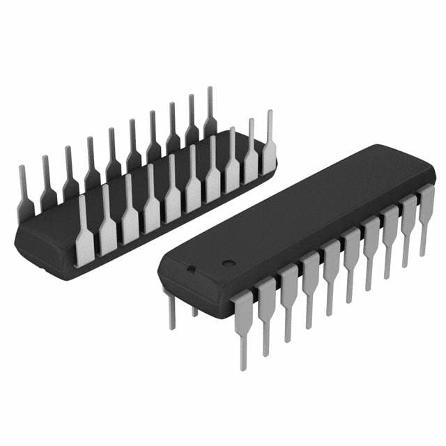
- Part No.:
- PCA9665N,112
- Manufacturer:
- NXP Semiconductors
- Category:
- Controllers
- Package:
- 20-DIP (0.300", 7.62mm)
- Datasheet:
-
 PCA9665N,112.pdf
- Description:
- IC CNTRLR PARALLEL/I2C 20-DIP
- Quantity:
- Payment:

- Shipping:

Inventory:4,634
Please send an inquiry. Send us your inquiry, and we will respond immediately.
Product details
Overview
PCA9665N,112 from NXP Semiconductors is a Fast-mode Plus (Fm+) parallel-bus-to-I²C-bus controller IC that bridges standard 8-bit parallel microcontrollers to the I²C-bus as either master or slave. It operates from 2.3 V to 3.6 V, delivers 1 Mbit/s I²C throughput with 25 mA SCL/SDA drive strength, and integrates a 68-byte buffer for efficient data transfer in industrial control and embedded systems.
For engineers reviewing the PCA9665N,112 datasheet, PCA9665N,112 pinout, PCA9665N,112 application, or PCA9665N,112 equivalent, key selection criteria include its DIP20 package compatibility, 5 V tolerant parallel I/Os, software reset capability, General Call support, and Fm+ timing compliance - all critical for legacy parallel bus integration and multi-master I²C expansion.
Technical Context
The PCA9665N,112 implements a fully autonomous I²C protocol engine with internal 28.5 MHz oscillator (±15% accuracy), eliminating external timing components. It handles arbitration, START/STOP generation, ACK/NACK, clock stretching, and timeout recovery without CPU intervention during transfers.
Its dual-mode operation supports Byte mode (single-byte transactions) and Buffered mode (up to 68 bytes per transaction), controlled via the MODE bit in I2CCON. Register access uses direct addressing (A0/A1) for four core registers and indirect addressing (via INDPTR) for seven configuration and status registers including I2CSCLL/I2CSCLH for precise SCL timing control.
Key Specifications
| Parameter | Value and Actual Design Meaning |
|---|---|
| I²C Speed Mode | Fast-mode Plus (Fm+): supports 1 Mbit/s operation with 25 mA SCL/SDA sink current for robust noise immunity on long traces |
| Supply Voltage | 2.3 V to 3.6 V: enables direct interface with 3.3 V logic systems while maintaining 5 V tolerance on parallel bus pins |
| Data Buffer Size | 68-byte FIFO: reduces CPU overhead by enabling burst reads/writes and minimizing interrupt frequency in buffered mode |
| Parallel Interface | 8-bit bidirectional data bus (D0–D7) with CE/WR/RD control: compatible with standard microcontroller address/data buses without glue logic |
| I²C Addressing | 7-bit slave address + General Call support (GC bit in I2CADR): allows broadcast commands and flexible multi-device topology |
| ESD Protection | 2000 V HBM, 200 V MM, 1000 V CDM: meets industrial-grade reliability requirements for board-level handling and field operation |
| Operating Temperature | −40 °C to +85 °C: qualified for extended industrial environments without derating |
Pinout & Package
PCA9665N,112 is supplied in a 20-pin plastic dual in-line package (DIP20), 300 mil width, with through-hole mounting and 2.54 mm pitch. Pin 1 is index-marked; pin 9 (i.c.) is internally connected and must be left floating.
| Pin/Terminal | Circuit Role | Design Meaning |
|---|---|---|
| D0–D7 | Parallel data bus I/O | Bidirectional 3-state interface to microcontroller data bus; D0 = LSB; all pins 5 V tolerant |
| i.c. | Internally connected | No external connection required; internally pulled LOW - must remain unconnected |
| VSS | Ground | Primary supply return; connects to system ground plane for stable reference and noise control |
| WR | Write strobe input | Active-LOW signal latching parallel data into addressed register on rising edge of WR or CE |
| RD | Read strobe input | Active-LOW signal enabling register contents onto D0–D7 bus; read cycle starts on falling edge of RD |
| CE | Chip enable input | Active-LOW global enable; places D0–D7 in high-impedance state when HIGH to prevent bus contention |
| A0, A1 | Register address inputs | Select among five direct-access registers (I2CSTA, INDPTR, I2CDAT, I2CCON, INDIRECT) via logic levels |
| INT | Interrupt output | Open-drain, active-LOW serial interrupt signaling I²C state changes; requires external pull-up resistor |
| RESET | Hardware reset input | Active-LOW asynchronous reset clearing internal registers and halting I²C state machine |
| SCL | I²C clock I/O | Open-drain bidirectional clock line; requires external pull-up; supports Fm+ timing with 25 mA drive |
| SDA | I²C data I/O | Open-drain bidirectional data line; requires external pull-up; supports Fm+ timing with 25 mA drive |
| VDD | Power supply | 2.3 V to 3.6 V main supply; decoupling capacitor (100 nF) recommended near pin for noise suppression |
Key Features
| Feature | Design Value |
|---|---|
| Integrated Fm+ I²C controller | Eliminates need for external timing components and firmware-based bit-banging; ensures full compliance with I²C Fast-mode Plus electrical specs |
| 68-byte transmit/receive buffer | Enables high-throughput I²C communication with minimal CPU polling or interrupt servicing - ideal for sensor arrays and display interfaces |
| Software reset via I2CPRESET register | Allows full functional reset of I²C state machine and registers without cycling VDD or asserting hardware RESET pin |
| 5 V tolerant parallel I/Os | Permits direct connection to legacy 5 V microcontrollers without level-shifting circuitry, reducing BOM count and layout complexity |
| I²C General Call recognition | Supports broadcast commands to multiple devices simultaneously, simplifying firmware updates and system-wide configuration |
Applications
| Industrial PLC I/O Expansion | Legacy MCU I²C Port Addition |
|---|---|
Use Scenario: Adding isolated analog/digital I/O modules to a 8051-based PLC backplane using parallel bus architecture. IC Role / Device Role / Timing Role: PCA9665N,112 acts as a dedicated I²C master bridge, converting parallel command packets into time-critical sensor read/write sequences over twisted-pair I²C bus. Use Value: Enables deterministic 1 Mbit/s I²C communication with 25 mA drive strength to overcome EMI in noisy factory environments, replacing custom FPGA logic. |
Use Scenario: Integrating EEPROM and temperature sensors into an existing Z80-based medical device without redesigning the CPU bus interface. IC Role / Device Role / Timing Role: PCA9665N,112 serves as a slave-configurable I²C peripheral, accepting parallel writes to configure its own 7-bit address and buffer depth before initiating I²C transactions. Use Value: Preserves original PCB layout and firmware structure while adding standardized I²C connectivity - no microcode modification required beyond register initialization. |
| Multi-Master Sensor Hub | Board-Level Trace Reduction |
Use Scenario: Coordinating multiple I²C sensor nodes (accelerometer, gyroscope, magnetometer) in an automotive ADAS module where multiple masters share one bus. IC Role / Device Role / Timing Role: PCA9665N,112 operates in multi-master mode with built-in arbitration logic, resolving bus conflicts and ensuring atomic read-modify-write cycles for shared configuration registers. Use Value: Guarantees reliable arbitration and collision recovery per I²C specification, avoiding data corruption during concurrent access by host MCU and safety monitor processor. |
Use Scenario: Replacing wide parallel interconnects between a mainboard and daughter card carrying I²C peripherals in a test equipment rack system. IC Role / Device Role / Timing Role: PCA9665N,112 converts 8-bit parallel data bursts into compact serial streams, reducing inter-board trace count from 16+ to just SCL/SDA/GND. Use Value: Cuts PCB layer count and routing congestion while maintaining full bandwidth - 68-byte buffering prevents bottlenecks during high-speed calibration data transfers. |
Equivalent & Alternatives
The following parts are listed as comparable options for similar parallel-to-I²C bridge applications.
| Alternative Part | Technical Difference | Application Difference | Selection Advice |
|---|---|---|---|
| PCA9564D,118 | Lacks Fm+ support (max 400 kbit/s), no 68-byte buffer (only 4-byte FIFO), lower SCL/SDA drive (3 mA), no General Call or software reset | Suitable only for low-speed, low-complexity I²C extensions; cannot replace PCA9665N,112 in 1 Mbit/s or multi-device broadcast scenarios | Select PCA9564D,118 only if cost sensitivity outweighs speed, buffer, and feature requirements - verify timing margins at 400 kbit/s |
| PCA9665PW,118 | Identical functionality and register map; differs only in TSSOP20 package (4.4 mm body width, surface-mount) | Requires PCB rework for SMT assembly; same electrical behavior and thermal profile as PCA9665N,112 in DIP20 | Choose PCA9665PW,118 for space-constrained designs needing surface-mount compatibility - no firmware or schematic changes needed |
Compared with PCA9564D,118, PCA9665N,112 delivers 2.5× higher I²C speed, 17× larger buffer, and Fm+-grade drive strength; versus PCA9665PW,118, it offers identical performance in through-hole DIP20 form factor for prototyping and legacy board upgrades.
Availability
PCA9665N,112 is available at Aetrix Electronics and suitable for industrial automation, medical instrumentation, and test equipment requiring stable component supply across long product lifecycles and mixed-technology PCB assemblies.
Supply support for PCA9665N,112 includes scheduled delivery planning, volume procurement assistance, BOM continuity management, traceable sourcing, and lifecycle availability coordination for OEM customers, industrial embedded developers, connected-device designers, and electronics production programs.
Manufacturer
NXP Semiconductors is a global semiconductor leader focused on secure connectivity solutions for automotive, industrial, and IoT applications, with deep expertise in interface and mixed-signal IC design.
The PCA9665N,112 belongs to NXP's I²C protocol controller product line, engineered specifically to simplify migration from parallel-bus architectures to standardized serial interconnects in resource-constrained embedded systems.
FAQ
What is the maximum I²C bus speed supported by the PCA9665N,112?
The PCA9665N,112 supports Fast-mode Plus (Fm+) operation up to 1 Mbit/s. This is achieved using its internal 28.5 MHz oscillator and 25 mA SCL/SDA drive capability, which ensures robust signal integrity on loaded or noisy buses. The actual speed depends on programmed I2CSCLL/I2CSCLH register values and external pull-up strength, but the PCA9665N,112 is fully compliant with Fm+ timing specifications.
Does the PCA9665N,112 require external crystals or timing components?
No, the PCA9665N,112 contains a trimmed internal 28.5 MHz oscillator with ±15% accuracy, eliminating the need for external crystals, capacitors, or RC networks. This oscillator powers all I²C timing functions including SCL generation, arbitration, and timeout detection - significantly reducing bill-of-materials and PCB area compared to discrete timing solutions.
How does the 68-byte buffer in the PCA9665N,112 improve system performance?
The 68-byte buffer in the PCA9665N,112 enables Buffered mode operation, allowing the host microcontroller to issue single read/write commands for up to 68 bytes instead of managing individual byte transfers. This reduces interrupt frequency, minimizes CPU overhead, and improves throughput - especially valuable in applications like sensor data logging or display memory updates where large sequential transfers occur.
Can the PCA9665N,112 operate with a 5 V parallel bus while powered at 3.3 V?
Yes, the PCA9665N,112 features 5 V tolerant parallel I/O pins (D0–D7, RD, WR, CE, A0, A1, RESET, INT), allowing direct connection to 5 V microcontrollers even when VDD is supplied at 2.3 V to 3.6 V. This eliminates level-shifter components and simplifies interfacing with legacy 5 V logic families while maintaining low-power operation.
What is the purpose of the i.c. pin on the PCA9665N,112 DIP20 package?
The i.c. pin (pin 9) on the PCA9665N,112 is internally connected and pulled LOW - it serves no external function and must be left unconnected (floating). Connecting it to any voltage or ground may cause undefined behavior or damage. This pin exists for package symmetry and die bonding purposes only; the PCA9665N,112 operates correctly with i.c. unconnected.
PCA9665N,112 Specifications
- Product attributes
- Attribute value
- Manufacturer:
- NXP Semiconductors
- Package/Case:
- 20-DIP (0.300", 7.62mm)
- Programmable:
- Not Verified
- Protocol:
- I2C
- Function:
- Controller
- Interface:
- Parallel
- Standards:
- -
- Voltage - Supply:
- 2.3V ~ 3.6V
- Current - Supply:
- 100µA
- Operating Temperature:
- -40°C ~ 85°C
- Supplier Device Package:
- 20-DIP
- Grade:
- -
- Qualification:
- -
PCA9665N,112 FAQ
1.How can I place an order for PCA9665N,112 through Aetrix?
Please submit a Request for Quotation (RFQ) for PCA9665N,112 on Aetrix. Our sales agent will provide a competitive quotation and guide you through the order confirmation once you accept the terms.
2.Are the price and stock information for PCA9665N,112 reliable?
The price and inventory of PCA9665N,112 are updated periodically and may fluctuate due to market conditions. Stock and pricing data are typically refreshed every 24 hours. Quotation validity for PCA9665N,112 is usually 5 days.
3.What payment methods are accepted for PCA9665N,112?
We accept Wire Transfer, PayPal, Credit Card, Western Union, MoneyGram, and Escrow for PCA9665N,112 transactions.
Note: Certain payment methods may incur a processing fee.
4.How is shipping managed for PCA9665N,112?
PCA9665N,112 orders can be shipped via leading logistics carriers, including DHL, UPS, FedEx, TNT, or Registered Mail.
Once your PCA9665N,112 order is processed, you will receive an email with the shipment details and tracking number.
Note: Tracking information may take up to 24 hours to appear. Express delivery typically takes 3–5 business days.
5.How can I obtain technical support or documentation for PCA9665N,112?
For technical support, including PCA9665N,112 datasheets, pinout diagrams, or application guidance, please contact our engineering support team. They can provide detailed documentation and assistance for your PCA9665N,112 requirements.
6.How does Aetrix verify that PCA9665N,112 is sourced from the original manufacturer or authorized distributors?
All PCA9665N,112 products on Aetrix are procured from qualified distributors and authorized channels. Our dedicated quality assurance team conducts strict verification, including traceability checks and, if necessary, third-party testing. This ensures that PCA9665N,112 meets industry standards.
7.What is the process for return or replacement of PCA9665N,112?
All PCA9665N,112 units undergo pre-shipment inspection (PSI). If there is an issue with PCA9665N,112, returns or replacements are accepted under the following conditions:
1.Quantity discrepancies, incorrect items, or visible external defects (such as breakage or corrosion), acknowledged by Aetrix.
2.The issue is reported within 90 days of delivery.
3.The PCA9665N,112 part is unused and in its original packaging.
Return procedure for PCA9665N,112:
1.Submit a request within 90 days.
2.Obtain a Return Material Authorization (RMA) from Aetrix.
PCA9665N,112 Tags

-
PTN5150AHXMP
NXP Semiconductors

-
USB3740B-AI9-TR
Microchip Technology

-
USB3740B-AI2-TR
Microchip Technology

-
USB3300-EZK-TR
Microchip Technology
-
USB3300-EZK
Microchip Technology

-
FUSB340TMX
onsemi

-
FUSB302BMPX
onsemi

-
DP83826IRHBR
Texas Instruments

-
MCP2518FDT-E/QBB
Microchip Technology
-
FUSB302MPX
onsemi

-
MCP2518FDT-E/SL
Microchip Technology

-
FT260Q-R
FTDI, Future Technology Devices International Ltd
Tech Hub

A practical engineering guide to 3.3V and 5V logic compatibility, input thresholds, resistor dividers, translator ICs, MOSFET level shifting, I2C pull-ups, timing limits and power-sequencing risks.

The 74HC595 uses push-pull logic outputs, while the TPIC6B595 uses 50 V open-drain DMOS sinks for higher-power loads. This guide compares timing, current limits, 3.3 V interfacing, load wiring, thermal…

The 74HC595 converts serial data into eight stable parallel outputs. This guide covers pin functions, shift and storage timing, OE and MR behavior, drive-current limits, cascading, voltage compatibilit…

A technical comparison of level-sensitive latches and edge-triggered flip-flops, covering timing windows, setup and hold limits, master–slave operation, time borrowing, race-through, HDL inference and…

A D latch stores one bit while Enable controls when data can pass. This reference covers gate-level operation, truth tables, transparency, setup and hold timing, LE versus OE, common ICs and practical …

An SR latch stores one bit through cross-coupled feedback. This engineering reference covers NOR and NAND implementations, truth tables, forbidden-state recovery, gated operation, switch debouncing, fa…

Latch circuits retain one bit through feedback. This technical reference covers SR and D latches, truth tables, transparency, timing limits, latch-versus-flip-flop behavior, applications and common log…

An engineering guide to LED driver operation, constant-current and constant-voltage outputs, linear and switching topologies, dimming, IC selection, calculations, replacement compatibility, and fault c…

Operational amplifier guide covering op amp basics, feedback, ideal vs real op amps, common configurations, buffer circuits, offset, bias current, gain-bandwidth, slew rate, rail-to-rail limits and sel…

Jumper cables guide covering safe connection order, red and black clamp placement, final ground connection, cable gauge, length, clamp quality, copper vs CCA cables, jump starter comparison and battery…


