
 My Inquiry
 My Account


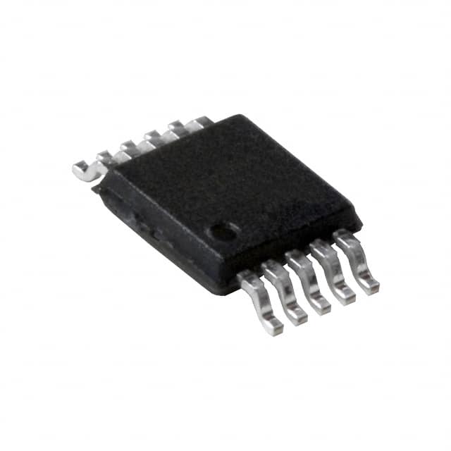
NXP Semiconductors PCF85363ATT1/AJ
- Part No.:
- PCF85363ATT1/AJ
- Manufacturer:
- NXP Semiconductors
- Category:
- Real Time Clocks
- Package:
- 10-TFSOP, 10-MSOP (0.118", 3.00mm Width)
- Datasheet:
-
 PCF85363ATT1/AJ.pdf
- Description:
- IC RTC CLK/CALENDAR I2C 10TSSOP
- Quantity:
- Payment:

- Shipping:

Inventory:1,968
Please send an inquiry. Send us your inquiry, and we will respond immediately.
Product details
Overview
PCF85363ATT1/AJ from NXP Semiconductors is a TSSOP10-packaged, I²C-compatible real-time clock/calendar IC with 64-byte battery-backed RAM, dual alarms, timestamp capture on power loss, and stopwatch mode supporting elapsed time up to 999,999 hours. It operates from 0.9 V to 5.5 V and draws only 0.28 µA typical at 3.0 V - enabling long-term backup in printers, network devices, and white goods.
For engineers reviewing the PCF85363ATT1/AJ datasheet, PCF85363ATT1/AJ pinout, PCF85363ATT1/AJ application, or PCF85363ATT1/AJ equivalent, key selection criteria include its TSSOP10 package with dedicated TS (timestamp/INTB) and CLK output pins, programmable oscillator load capacitance (6/7/12.5 pF), and dual interrupt outputs (INTA open-drain, INTB push-pull) for alarm and periodic event signaling.
Technical Context
The PCF85363ATT1/AJ implements a fully autonomous RTC core with BCD-coded time registers (100th seconds through years), auto-incrementing I²C address pointer, and hardware freeze-on-read to prevent carry corruption during time reads. Its oscillator circuit supports configurable crystal load capacitance and includes offset calibration for ±10 ppm accuracy tuning.
It features three timestamp registers triggered by battery switchover or external TS input, two independent alarm engines (Alarm 1: sec–month; Alarm 2: min–weekday), and a watchdog timer with programmable timeout. The device switches seamlessly between VDD and VBAT supply without software intervention, maintaining time and RAM contents during main power loss.
Key Specifications
| Parameter | Value and Actual Design Meaning |
|---|---|
| Supply Voltage Range | 0.9 V to 5.5 V - enables direct interface with 1.8 V, 3.3 V, and 5 V host systems without level shifters. |
| Quiescent Current | 0.28 µA typical at VDD = 3.0 V - extends battery life to >10 years on CR2032 in backup mode. |
| I²C Bus Speed | Up to 400 kHz - compatible with standard/fast-mode I²C controllers across microcontrollers and SoCs. |
| RAM Capacity | 64 bytes battery-backed - retains configuration, logs, or user data during power failure without external EEPROM. |
| Timestamp Triggers | Three independent timestamp registers - capture precise time-of-event for battery switchover, mechanical switch detection, or external TS pulse. |
| Alarm Outputs | Two independent alarms with configurable enable bits - support simultaneous wake-up, notification, and scheduling without CPU polling. |
| Clock Output | Programmable CLK pin (32.768 kHz to 1 Hz) - drives external logic, MCU timers, or low-power peripherals directly. |
Pinout & Package
PCF85363ATT1/AJ uses a plastic thin shrink small outline package (TSSOP10) with 0.5 mm pitch, 3 mm body width, and exposed pad (not electrically connected). Pin 1 is marked by index area; pin numbering follows standard TSSOP convention.
| Pin/Terminal | Circuit Role | Design Meaning |
|---|---|---|
| 1 OSCI | Oscillator input | Connects to one terminal of 32.768 kHz quartz crystal; internal bias circuit enables direct crystal drive. |
| 2 OSCO | Oscillator output | Drives second crystal terminal; forms Pierce oscillator with internal inverter and configurable CL (6/7/12.5 pF). |
| 3 VBAT | Battery backup supply | Accepts coin-cell or supercapacitor; automatically powers RTC/RAM when VDD drops below VTH (~1.1 V). |
| 4 TS (CLK/INTB) | Timestamp input / CLK output / INTB output | Configurable multifunction pin: timestamp trigger (input), programmable clock (push-pull output), or interrupt (INTB). |
| 5 VSS | Ground | Primary reference for all analog/digital circuits; die paddle must be isolated but may be soldered for thermal relief. |
| 6 SDA | I²C serial data | Open-drain bidirectional line; requires external pull-up; supports multi-master arbitration and clock stretching. |
| 7 SCL | I²C serial clock | Input-only clock line; synchronizes all I²C transfers; tolerant of slow edges due to Schmitt-trigger input. |
| 8 CLK | Programmable clock output | Push-pull output delivering selectable frequencies (32.768 kHz to 1 Hz); usable as system timing reference. |
| 9 INTA (CLK) | Interrupt output / CLK output | Open-drain interrupt (INTA) or alternate CLK output; configured via INTAPM[1:0] register bits. |
| 10 VDD | Main supply voltage | Primary power source (0.9–5.5 V); powers digital core, I²C interface, and oscillator; enables automatic switchover to VBAT. |
Key Features
| Feature | Design Value |
|---|---|
| Stopwatch mode | Elapsed time counter from 100th seconds to 999,999 hours - eliminates need for external counters in data loggers and test equipment. |
| Automatic battery switchover | No software or external circuitry required - seamless transition preserves time, alarms, and RAM contents during VDD interruption. |
| Dual independent interrupts | INTA (open-drain) and INTB (push-pull) with configurable polarity - enables concurrent event handling (e.g., alarm + timestamp) without GPIO contention. |
| Crystal calibration offset register | 8-bit programmable offset (±127 ppm range) - compensates for crystal aging, temperature drift, or PCB parasitics without hardware changes. |
| BCD time registers with freeze-on-read | Hardware freezes all time counters during I²C read - guarantees atomic access to consistent hh:mm:ss.dd values without software locking. |
Applications
| Printer Power Loss Logging | Network Equipment Time Sync |
|---|---|
|
Use Scenario: Captures exact timestamp when mains power fails in laser printers or MFPs, enabling accurate job accounting and fault diagnostics. IC Role / Device Role / Timing Role: PCF85363ATT1/AJ acts as autonomous timestamp recorder triggered by VDD drop, storing time-of-failure in battery-backed RAM. Use Value: Eliminates reliance on host MCU uptime; ensures reliable logging even if main processor crashes or resets during brownout. |
Use Scenario: Maintains accurate wall-clock time across reboots and firmware updates in Ethernet switches and routers with no GPS or NTP dependency. IC Role / Device Role / Timing Role: PCF85363ATT1/AJ serves as primary time-of-day source, synchronized via I²C to host processor at boot and updated periodically. Use Value: Enables consistent syslog timestamps, certificate validity checks, and scheduled maintenance windows independent of network connectivity. |
| White Goods Energy Monitoring | Digital Voice Recorder Session Tracking |
|
Use Scenario: Logs cumulative run time and cycle start/end times in refrigerators, washing machines, and dishwashers for predictive maintenance. IC Role / Device Role / Timing Role: PCF85363ATT1/AJ operates in stopwatch mode to track motor runtime, while RTC mode records calendar dates for service intervals. Use Value: Provides tamper-resistant, battery-backed usage history that survives full power cycles and firmware reflashes. |
Use Scenario: Assigns precise start/end timestamps to audio recordings in portable voice recorders, enabling searchable playback and metadata export. IC Role / Device Role / Timing Role: PCF85363ATT1/AJ supplies BCD-formatted time/date to recording firmware via I²C and triggers timestamp capture on record button press. Use Value: Delivers sub-second accuracy (100th seconds) without requiring high-frequency MCU timers or external precision clocks. |
Equivalent & Alternatives
The following parts are listed as comparable options for similar real-time clock applications.
| Alternative Part | Technical Difference | Application Difference | Selection Advice |
|---|---|---|---|
| PCF85363ATT1/AZ | Identical functionality and pinout; same TSSOP10 package; drop-in replacement per NXP PCN 202104008A. | No functional difference; intended for new designs after discontinuation notice for PCF85363ATT1/AJ. | Select PCF85363ATT1/AZ for long-term design continuity and guaranteed availability beyond 2021 discontinuation date. |
| DS3231SN#T&R | Higher accuracy (±2 ppm vs. ±10 ppm typical), integrated TCXO, but no stopwatch mode or timestamp registers. | Preferred where absolute time accuracy is critical (e.g., scientific instruments); unsuitable for elapsed-time logging or power-loss event capture. | Choose DS3231SN#T&R only when sub-ppm stability outweighs need for PCF85363ATT1/AJ's stopwatch, triple timestamp, and flexible alarm features. |
Compared with PCF85363ATT1/AJ, PCF85363ATT1/AZ offers identical electrical and functional behavior with assured supply chain continuity, while DS3231SN#T&R trades stopwatch capability and timestamp flexibility for superior oscillator stability - making it suitable only for pure high-accuracy RTC use cases.
Availability
PCF85363ATT1/AJ is available at Aetrix Electronics and suitable for printers, network equipment, and white goods requiring stable component supply with long-term industrial temperature support (−40 °C to +85 °C).
Supply support for PCF85363ATT1/AJ includes scheduled delivery planning, volume procurement assistance, BOM continuity management, traceable sourcing, and lifecycle availability coordination for OEM customers, industrial embedded developers, connected-device designers, and electronics production programs.
Manufacturer
NXP Semiconductors is a global semiconductor leader focused on secure connectivity solutions for automotive, industrial, and IoT applications, with deep expertise in low-power mixed-signal design.
The PCF85363A product line delivers ultra-low-power RTCs optimized for battery-backed operation, timestamp integrity, and system-level event logging - targeting applications where time persistence and power resilience are non-negotiable.
FAQ
What is the primary function of the TS (CLK/INTB) pin on the PCF85363ATT1/AJ?
The TS (CLK/INTB) pin on the PCF85363ATT1/AJ is a multifunction terminal supporting three modes: timestamp input (triggered by falling edge), programmable clock output (32.768 kHz to 1 Hz), or interrupt output (INTB, push-pull). Its behavior is controlled by the TSPM[1:0] bits in the Pin_IO register (27h), allowing dynamic reconfiguration without hardware change. This flexibility makes PCF85363ATT1/AJ adaptable to diverse timing and event-capture requirements.
Does the PCF85363ATT1/AJ support both 12-hour and 24-hour time formats?
Yes, the PCF85363ATT1/AJ supports both 12-hour and 24-hour time formats. The format is selected via the 12_24 bit in the Oscillator register (25h): when set to 1, hours are encoded in 12-hour mode with AMPM bit indicating AM/PM; when cleared to 0, hours use 24-hour format. All time registers (including alarms and timestamps) follow the selected mode, and the PCF85363ATT1/AJ handles leap-year compensation automatically in RTC mode.
How does the PCF85363ATT1/AJ handle time reads to prevent corruption during carry events?
The PCF85363ATT1/AJ prevents time corruption during carry events by freezing all RTC time registers (00h–07h) at the start of any I²C read transaction. This hardware freeze ensures that sequential reads of seconds, minutes, hours, etc., return a consistent snapshot - eliminating race conditions caused by rollovers mid-read. Engineers must read or write the full time/date block (100th seconds through years) in a single I²C burst to maintain atomicity, a requirement explicitly enforced by the PCF85363ATT1/AJ's architecture.
Can the PCF85363ATT1/AJ operate solely on battery power without VDD present?
Yes, the PCF85363ATT1/AJ can operate continuously on VBAT alone when VDD is absent or below the switchover threshold (~1.1 V). In this mode, it maintains real-time clock operation, alarm functionality, 64-byte RAM retention, and timestamp capture - drawing only 0.28 µA typical. The device automatically resumes VDD-supplied operation when main power returns, with no reset or configuration loss. This behavior is intrinsic to the PCF85363ATT1/AJ's battery switchover circuit and requires no external diodes or control logic.
What crystal load capacitance options does the PCF85363ATT1/AJ support?
The PCF85363ATT1/AJ supports three selectable crystal load capacitances: 6 pF, 7 pF, and 12.5 pF - configured via the CL[1:0] bits in the Oscillator register (25h). This allows optimization for common 32.768 kHz tuning fork crystals without external load capacitors, reducing BOM count and PCB area. The selection directly affects oscillation stability and startup time, with higher CL values generally improving robustness across temperature and voltage variations in the PCF85363ATT1/AJ's oscillator circuit.
PCF85363ATT1/AJ Specifications
- Product attributes
- Attribute value
- Manufacturer:
- NXP Semiconductors
- Series:
- -
- Package/Case:
- 10-TFSOP, 10-MSOP (0.118", 3.00mm Width)
- Packaging:
- Tape & Reel (TR)
- Product Status:
- Obsolete
- Programmable:
- Not Verified
- Type:
- Clock/Calendar
- Features:
- Alarm, Leap Year, Watchdog Timer
- Memory Size:
- 64B
- Time Format:
- HH:MM:SS:hh (12/24 hr)
- Date Format:
- YY-MM-DD-dd
- Interface:
- I2C, 2-Wire Serial
- Voltage - Supply:
- 0.9V ~ 5.5V
- Voltage - Supply, Battery:
- 0.9V ~ 5.5V
- Current - Timekeeping (Max):
- 0.885µA @ 3.3V
- Operating Temperature:
- -40°C ~ 85°C
- Mounting Type:
- Surface Mount
- Grade:
- -
- Qualification:
- -
- Supplier Device Package:
- 10-TSSOP
PCF85363ATT1/AJ FAQ
1.How can I place an order for PCF85363ATT1/AJ through Aetrix?
Please submit a Request for Quotation (RFQ) for PCF85363ATT1/AJ on Aetrix. Our sales agent will provide a competitive quotation and guide you through the order confirmation once you accept the terms.
2.Are the price and stock information for PCF85363ATT1/AJ reliable?
The price and inventory of PCF85363ATT1/AJ are updated periodically and may fluctuate due to market conditions. Stock and pricing data are typically refreshed every 24 hours. Quotation validity for PCF85363ATT1/AJ is usually 5 days.
3.What payment methods are accepted for PCF85363ATT1/AJ?
We accept Wire Transfer, PayPal, Credit Card, Western Union, MoneyGram, and Escrow for PCF85363ATT1/AJ transactions.
Note: Certain payment methods may incur a processing fee.
4.How is shipping managed for PCF85363ATT1/AJ?
PCF85363ATT1/AJ orders can be shipped via leading logistics carriers, including DHL, UPS, FedEx, TNT, or Registered Mail.
Once your PCF85363ATT1/AJ order is processed, you will receive an email with the shipment details and tracking number.
Note: Tracking information may take up to 24 hours to appear. Express delivery typically takes 3–5 business days.
5.How can I obtain technical support or documentation for PCF85363ATT1/AJ?
For technical support, including PCF85363ATT1/AJ datasheets, pinout diagrams, or application guidance, please contact our engineering support team. They can provide detailed documentation and assistance for your PCF85363ATT1/AJ requirements.
6.How does Aetrix verify that PCF85363ATT1/AJ is sourced from the original manufacturer or authorized distributors?
All PCF85363ATT1/AJ products on Aetrix are procured from qualified distributors and authorized channels. Our dedicated quality assurance team conducts strict verification, including traceability checks and, if necessary, third-party testing. This ensures that PCF85363ATT1/AJ meets industry standards.
7.What is the process for return or replacement of PCF85363ATT1/AJ?
All PCF85363ATT1/AJ units undergo pre-shipment inspection (PSI). If there is an issue with PCF85363ATT1/AJ, returns or replacements are accepted under the following conditions:
1.Quantity discrepancies, incorrect items, or visible external defects (such as breakage or corrosion), acknowledged by Aetrix.
2.The issue is reported within 90 days of delivery.
3.The PCF85363ATT1/AJ part is unused and in its original packaging.
Return procedure for PCF85363ATT1/AJ:
1.Submit a request within 90 days.
2.Obtain a Return Material Authorization (RMA) from Aetrix.
PCF85363ATT1/AJ Tags

-
MCP7940N-I/SN
Microchip Technology
-
MCP7940MT-I/MNY
Microchip Technology

-
PCF85063ATL/1,118
NXP USA Inc.
-
MCP7940NT-I/SN
Microchip Technology

-
MCP7940NT-I/MS
Microchip Technology
-
MCP7940N-I/MS
Microchip Technology
-
PCF85063AT/AY
NXP USA Inc.

-
PCF85063TP/1Z
NXP Semiconductors

-
PCF85063ATT/AJ
NXP USA Inc.
-
MCP7940NT-E/SN
Microchip Technology
-
MCP7940NT-I/MNY
Microchip Technology
-
MCP79400T-I/SN
Microchip Technology
Tech Hub

A practical engineering guide to 3.3V and 5V logic compatibility, input thresholds, resistor dividers, translator ICs, MOSFET level shifting, I2C pull-ups, timing limits and power-sequencing risks.

The 74HC595 uses push-pull logic outputs, while the TPIC6B595 uses 50 V open-drain DMOS sinks for higher-power loads. This guide compares timing, current limits, 3.3 V interfacing, load wiring, thermal…

The 74HC595 converts serial data into eight stable parallel outputs. This guide covers pin functions, shift and storage timing, OE and MR behavior, drive-current limits, cascading, voltage compatibilit…

A technical comparison of level-sensitive latches and edge-triggered flip-flops, covering timing windows, setup and hold limits, master–slave operation, time borrowing, race-through, HDL inference and…

A D latch stores one bit while Enable controls when data can pass. This reference covers gate-level operation, truth tables, transparency, setup and hold timing, LE versus OE, common ICs and practical …

An SR latch stores one bit through cross-coupled feedback. This engineering reference covers NOR and NAND implementations, truth tables, forbidden-state recovery, gated operation, switch debouncing, fa…

Latch circuits retain one bit through feedback. This technical reference covers SR and D latches, truth tables, transparency, timing limits, latch-versus-flip-flop behavior, applications and common log…

An engineering guide to LED driver operation, constant-current and constant-voltage outputs, linear and switching topologies, dimming, IC selection, calculations, replacement compatibility, and fault c…

Operational amplifier guide covering op amp basics, feedback, ideal vs real op amps, common configurations, buffer circuits, offset, bias current, gain-bandwidth, slew rate, rail-to-rail limits and sel…

Jumper cables guide covering safe connection order, red and black clamp placement, final ground connection, cable gauge, length, clamp quality, copper vs CCA cables, jump starter comparison and battery…


