
 My Inquiry
 My Account


Texas Instruments PCI1450GJG
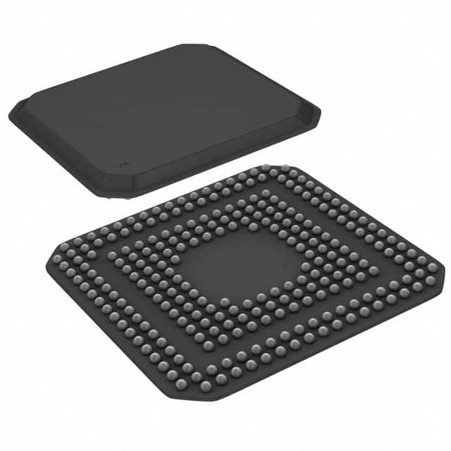
- Part No.:
- PCI1450GJG
- Manufacturer:
- Texas Instruments
- Category:
- Controllers
- Package:
- 257-LFBGA
- Datasheet:
-
 PCI1450GJG.pdf
- Description:
- IC PC CARD CNTRLR 257-BGA
- Quantity:
- Payment:

- Shipping:

Inventory:1,568
Please send an inquiry. Send us your inquiry, and we will respond immediately.
Product details
Overview
PCI1450GJG from Texas Instruments is a dual-slot PC Card controller IC bridging 32-bit PCI bus to 16-bit PC Card and 32-bit CardBus interfaces. It supports hot insertion/removal, 132 MB/s burst transfers, ACPI 1.0 and PCI 2.1/2.2 compliance, and integrated Zoomed Video (ZV) path with 23 dedicated pins. Used in notebook/desktop add-in cards for legacy expansion.
For engineers reviewing the PCI1450GJG datasheet, PCI1450GJG pinout, PCI1450GJG application, or PCI1450GJG equivalent, key selection considerations include ExCA register compatibility with Intel 82365SL-DF, dual-socket power management (D3 cold wake-up), programmable interrupt routing (4 modes), ZV signal buffering, and 257-pin Micro-Star BGA package mechanical constraints.
Technical Context
The PCI1450GJG implements a PCI-to-CardBus bridge with two independent socket controllers, each supporting full 32-bit PCI cycles for 8-/16-/32-bit card access. Its pipeline architecture enables sustained bursting, while internal buffering isolates card signals for hot-swap safety.
It integrates a programmable interrupt subsystem with 8 IRQMUX outputs (configurable to 15 ISA IRQs), four GPIOs, and serial EEPROM interface for subsystem ID loading. The ZV path operates at pixel clock rates up to 27 MHz with dedicated PCLK, SCLK, LRCLK, SDATA, and sync signals (HREF/VSYNC).
Key Specifications
| Parameter | Value and Actual Design Meaning |
|---|---|
| PCI Interface | 32-bit, 33 MHz compliant with PCI Local Bus Spec Rev 2.1/2.2; supports master/slave operation and LOCK protocol |
| Card Support | Two independent sockets: mix-and-match 5-V/3.3-V 16-bit PC Cards and 3.3-V CardBus cards |
| Data Throughput | 132 MB/s burst transfer rate on both PCI and CardBus buses via pipelined data-path logic |
| Power Management | ACPI 1.0 and PCI Power Management Spec compliant; supports D3cold wake-up via PME and SUSPEND signals |
| Zoomed Video | Internally buffered ZV path with 23 dedicated pins; meets CardBus loading specs without external components |
| Interrupt Architecture | Four configurable modes: Serial ISA/Serial PCI, Serial ISA/Parallel PCI, Parallel ISA/Parallel PCI, Parallel PCI Only |
| Package | 257-pin Micro-Star Ball Grid Array (BGA); 27 mm × 27 mm footprint, 1.27 mm ball pitch |
Pinout & Package
Packaged in a 257-pin Micro-Star BGA (GJG suffix), this device uses a 27 mm × 27 mm body with 1.27 mm ball pitch. Pin assignments follow Table 2 (GJG terminals) in SCPS044, grouping signals into PCI, CardBus A/B, Zoomed Video, power, and multifunction I/O categories.
| Pin/Terminal | Circuit Role | Design Meaning |
|---|---|---|
| AD31–AD0 | PCI address/data multiplexed bus | 32-bit bidirectional bus carrying address during phase 1, data during phase 2; requires external latching for synchronous capture |
| C/BE3–C/BE0 | PCI command/byte enable | Defines transaction type (e.g., memory read/write) in address phase; selects active bytes (0–3) in data phase |
| ZV_PCLK, ZV_SCLK, ZV_LRCLK | Zoomed Video timing | Provides pixel clock, serial clock, and left/right frame sync for direct VGA controller interfacing without glue logic |
| IRQMUX0–IRQMUX7 | Programmable interrupt outputs | Eight outputs individually mappable to 15 ISA IRQ lines; secondary functions include INTB, RI_OUT, and DMA request/grant |
| GPIO0/LEDA1, GPIO1/LEDA2 | General-purpose I/O / LED drivers | Configurable as inputs/outputs; drive socket activity LEDs directly with current-limited open-drain outputs |
Key Features
| Feature | Design Value |
|---|---|
| ExCA Register Compatibility | Fully compatible with Intel 82365SL-DF register map, enabling drop-in driver reuse in legacy PCMCIA systems |
| Distributed DMA Support | Enables peer-to-peer DMA between PC Cards and PCI peripherals without CPU intervention, reducing host overhead |
| 90 µs Noise Immunity | Card detect lines tolerate >90 µs of electrical noise, preventing false hot-plug detection in electrically noisy laptop chassis |
| Internal Ring Oscillator | Eliminates need for external clock source on CLOCK/DATA/LATCH lines when driving TI TPS2206 dual power switch |
| PCI CLKRUN Interface | Dedicated CLKRUN pin allows system-level clock gating for dynamic power reduction during idle PCI periods |
| VGA Palette Memory Decoding | Hardware support for subtractive decoding of VGA palette I/O space (3C0h–3CCh), simplifying video subsystem integration |
Applications
| Mobile Notebook Expansion | Desktop Docking Station |
|---|---|
Use Scenario: Adding legacy PC Card modems, network adapters, or SCSI controllers to ultraportable notebooks with no native CardBus slot. IC Role / Device Role / Timing Role: PCI-to-CardBus bridge providing hot-plug-safe socket control, ZV path for integrated webcam video, and serialized IRQ routing to conserve chipset interrupt resources. Use Value: Enables single-chip support for both 16-bit and 32-bit cards while maintaining ACPI-compliant suspend/resume behavior across all power states (D0–D3cold). |
Use Scenario: High-bandwidth docking station connecting multiple PC Cards (e.g., FireWire + CompactFlash + audio codec) to desktop motherboard via PCI slot. IC Role / Device Role / Timing Role: Dual-socket controller managing independent power sequencing, distributed DMA for simultaneous card transfers, and parallel PCI interrupt aggregation (INTA/INTB). Use Value: Delivers 132 MB/s aggregate throughput across sockets with zero wait-state bursts, eliminating bottlenecks in multi-card data acquisition systems. |
| Industrial Data Acquisition | Medical Imaging Peripheral |
Use Scenario: Ruggedized field instrument using PC Card-based GPS receivers and cellular modems in harsh EMI environments. IC Role / Device Role / Timing Role: Bridge with 90 µs card-detect noise immunity, SUSPEND signaling for low-power sleep, and ring-indicate output for modem call alerts. Use Value: Prevents spurious card-removal interrupts in electrically noisy industrial settings, ensuring reliable hot-swap operation over 10,000+ insertions. |
Use Scenario: Portable ultrasound device requiring real-time video streaming from CardBus-based image sensor to host via Zoomed Video interface. IC Role / Device Role / Timing Role: ZV path controller buffering YUV7:0 and UV6:0 pixel streams, synchronizing HREF/VSYNC to host VGA controller, and managing ZV power domain isolation. Use Value: Guarantees CardBus-compliant ZV signal loading without external buffers, enabling medical-grade video latency < 16 ms at 640×480@30 fps. |
Equivalent & Alternatives
The following parts are listed as comparable options for similar PC Card controller applications.
| Alternative Part | Technical Difference | Application Difference | Selection Advice |
|---|---|---|---|
| PCI1225GJG | Single-socket controller; lacks Zoomed Video interface and 4 GPIOs; supports only CardBus (no 16-bit PC Card) | Suitable for cost-sensitive embedded designs needing only one high-speed socket without legacy card support | Select when dual-socket capability, ZV, or 16-bit PC Card backward compatibility are unnecessary |
| YUKON-PCI1450 | Second-source variant with identical pinout and register set; same 257-pin GJG package and thermal profile | Drop-in replacement for supply chain diversification; identical firmware and driver compatibility | Choose for dual-sourcing assurance without design or qualification changes |
Compared with PCI1225GJG, the PCI1450GJG adds dual-socket flexibility and ZV acceleration; compared with YUKON-PCI1450, it offers identical functionality but from Texas Instruments' validated production line with full documentation traceability.
Availability
PCI1450GJG is available at Aetrix Electronics and suitable for mobile notebook expansion, industrial data acquisition, and medical imaging peripherals requiring stable component supply across extended product lifecycles.
Supply support for PCI1450GJG includes scheduled delivery planning, volume procurement assistance, BOM continuity management, traceable sourcing, and lifecycle availability coordination for OEM customers, industrial embedded developers, connected-device designers, and electronics production programs.
Manufacturer
Texas Instruments is a global semiconductor company founded in 1930, specializing in analog, embedded processing, and connectivity solutions for industrial, automotive, and computing markets.
The PCI1450GJG belongs to TI's PC Card bridge product line, designed specifically to enable seamless integration of legacy PCMCIA peripherals into modern PCI-based systems while meeting PC 98/99 and ACPI power management requirements.
FAQ
What is the primary function of the PCI1450GJG in a system architecture?
The PCI1450GJG serves as a PCI-to-CardBus bridge IC, enabling host systems with a 32-bit PCI bus to interface with two independent PC Card sockets-supporting both legacy 16-bit PC Cards and 32-bit CardBus devices. It handles protocol translation, power management, interrupt routing, and Zoomed Video signal buffering, making it essential for notebook expansion cards and docking stations. The PCI1450GJG integrates all necessary logic to eliminate external glue components in compliant designs.
Does the PCI1450GJG support hot insertion and removal of PC Cards?
Yes, the PCI1450GJG fully supports hot insertion and removal through internal signal buffering, advanced noise immunity (90 µs on card detect lines), and robust power-switch control via its 3-line serial interface to TI TPS2206. All card signals are isolated during insertion/removal events, and the device maintains stable register state during transitions between D0 and D3 power states. This ensures reliable operation in portable systems where users frequently swap modems, network adapters, or storage cards.
How does the Zoomed Video (ZV) interface of the PCI1450GJG differ from standard video I/O?
The PCI1450GJG's ZV interface provides a dedicated, internally buffered 23-pin path-including PCLK, SCLK, LRCLK, SDATA, HREF, VSYNC, and YUV/UV pixel buses-that connects directly to VGA controllers without external drivers or level shifters. Unlike generic video I/O, this path meets CardBus loading specifications, guarantees timing compliance, and offloads pixel data handling from the CPU via DMA. The PCI1450GJG manages ZV power domains separately, enabling low-latency video streaming in medical and industrial imaging applications.
Is the PCI1450GJG pin-compatible with the Intel 82365SL-DF controller?
The PCI1450GJG is ExCA register-compatible with the Intel 82365SL-DF, meaning software drivers and configuration logic can be reused-but it is not pin-compatible due to architectural differences: the PCI1450GJG uses a 257-pin Micro-Star BGA package with integrated ZV signals and dual-socket control, whereas the 82365SL-DF is a 128-pin PQFP device supporting only single-socket 16-bit PC Cards. Hardware redesign is required, though firmware migration is simplified by register mapping alignment.
What power management features does the PCI1450GJG implement per ACPI 1.0 and PCI specifications?
The PCI1450GJG implements full ACPI 1.0 and PCI Power Management Specification compliance, including D0–D3cold states, PME wake-up from D3cold via RI_OUT/PME pin, SUSPEND signaling, CLKRUN-driven clock gating, and hardware-assisted D3 entry/exit sequencing. It supports PCI bus lock (LOCK), distributed DMA for low-CPU wake events, and programmable D3 status reporting. These features allow host OS power managers to coordinate deep sleep states across PC Cards and the bridge itself-critical for battery life in mobile platforms using the PCI1450GJG.
PCI1450GJG Specifications
- Product attributes
- Attribute value
- Manufacturer:
- Texas Instruments
- Package/Case:
- 257-LFBGA
- Programmable:
- Not Verified
- Protocol:
- -
- Function:
- -
- Interface:
- -
- Standards:
- -
- Voltage - Supply:
- -
- Current - Supply:
- -
- Operating Temperature:
- -
- Supplier Device Package:
- 257-BGA MICROSTAR (16x16)
- Grade:
- -
- Qualification:
- -
PCI1450GJG FAQ
1.How can I place an order for PCI1450GJG through Aetrix?
Please submit a Request for Quotation (RFQ) for PCI1450GJG on Aetrix. Our sales agent will provide a competitive quotation and guide you through the order confirmation once you accept the terms.
2.Are the price and stock information for PCI1450GJG reliable?
The price and inventory of PCI1450GJG are updated periodically and may fluctuate due to market conditions. Stock and pricing data are typically refreshed every 24 hours. Quotation validity for PCI1450GJG is usually 5 days.
3.What payment methods are accepted for PCI1450GJG?
We accept Wire Transfer, PayPal, Credit Card, Western Union, MoneyGram, and Escrow for PCI1450GJG transactions.
Note: Certain payment methods may incur a processing fee.
4.How is shipping managed for PCI1450GJG?
PCI1450GJG orders can be shipped via leading logistics carriers, including DHL, UPS, FedEx, TNT, or Registered Mail.
Once your PCI1450GJG order is processed, you will receive an email with the shipment details and tracking number.
Note: Tracking information may take up to 24 hours to appear. Express delivery typically takes 3–5 business days.
5.How can I obtain technical support or documentation for PCI1450GJG?
For technical support, including PCI1450GJG datasheets, pinout diagrams, or application guidance, please contact our engineering support team. They can provide detailed documentation and assistance for your PCI1450GJG requirements.
6.How does Aetrix verify that PCI1450GJG is sourced from the original manufacturer or authorized distributors?
All PCI1450GJG products on Aetrix are procured from qualified distributors and authorized channels. Our dedicated quality assurance team conducts strict verification, including traceability checks and, if necessary, third-party testing. This ensures that PCI1450GJG meets industry standards.
7.What is the process for return or replacement of PCI1450GJG?
All PCI1450GJG units undergo pre-shipment inspection (PSI). If there is an issue with PCI1450GJG, returns or replacements are accepted under the following conditions:
1.Quantity discrepancies, incorrect items, or visible external defects (such as breakage or corrosion), acknowledged by Aetrix.
2.The issue is reported within 90 days of delivery.
3.The PCI1450GJG part is unused and in its original packaging.
Return procedure for PCI1450GJG:
1.Submit a request within 90 days.
2.Obtain a Return Material Authorization (RMA) from Aetrix.
PCI1450GJG Tags

-
PTN5150AHXMP
NXP Semiconductors

-
USB3740B-AI9-TR
Microchip Technology

-
USB3740B-AI2-TR
Microchip Technology

-
USB3300-EZK-TR
Microchip Technology
-
USB3300-EZK
Microchip Technology

-
FUSB340TMX
onsemi

-
FUSB302BMPX
onsemi

-
DP83826IRHBR
Texas Instruments

-
MCP2518FDT-E/QBB
Microchip Technology
-
FUSB302MPX
onsemi

-
MCP2518FDT-E/SL
Microchip Technology

-
FT260Q-R
FTDI, Future Technology Devices International Ltd
Tech Hub

A practical engineering guide to 3.3V and 5V logic compatibility, input thresholds, resistor dividers, translator ICs, MOSFET level shifting, I2C pull-ups, timing limits and power-sequencing risks.

The 74HC595 uses push-pull logic outputs, while the TPIC6B595 uses 50 V open-drain DMOS sinks for higher-power loads. This guide compares timing, current limits, 3.3 V interfacing, load wiring, thermal…

The 74HC595 converts serial data into eight stable parallel outputs. This guide covers pin functions, shift and storage timing, OE and MR behavior, drive-current limits, cascading, voltage compatibilit…

A technical comparison of level-sensitive latches and edge-triggered flip-flops, covering timing windows, setup and hold limits, master–slave operation, time borrowing, race-through, HDL inference and…

A D latch stores one bit while Enable controls when data can pass. This reference covers gate-level operation, truth tables, transparency, setup and hold timing, LE versus OE, common ICs and practical …

An SR latch stores one bit through cross-coupled feedback. This engineering reference covers NOR and NAND implementations, truth tables, forbidden-state recovery, gated operation, switch debouncing, fa…

Latch circuits retain one bit through feedback. This technical reference covers SR and D latches, truth tables, transparency, timing limits, latch-versus-flip-flop behavior, applications and common log…

An engineering guide to LED driver operation, constant-current and constant-voltage outputs, linear and switching topologies, dimming, IC selection, calculations, replacement compatibility, and fault c…

Operational amplifier guide covering op amp basics, feedback, ideal vs real op amps, common configurations, buffer circuits, offset, bias current, gain-bandwidth, slew rate, rail-to-rail limits and sel…

Jumper cables guide covering safe connection order, red and black clamp placement, final ground connection, cable gauge, length, clamp quality, copper vs CCA cables, jump starter comparison and battery…


