
 My Inquiry
 My Account


Texas Instruments PCI2050BPDVG4
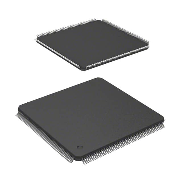
- Part No.:
- PCI2050BPDVG4
- Manufacturer:
- Texas Instruments
- Category:
- Specialized
- Package:
- 208-LQFP
- Datasheet:
-
 PCI2050BPDVG4.pdf
- Description:
- IC INTERFACE SPECIALIZED 208LQFP
- Quantity:
- Payment:

- Shipping:

Inventory:4,044
Please send an inquiry. Send us your inquiry, and we will respond immediately.
Product details
Overview
PCI2050BPDVG4 from Texas Instruments is a PCI-to-PCI bridge IC enabling high-performance interconnection between two 32-bit, 66-MHz PCI buses. It supports concurrent bidirectional burst transfers, write combining, and internal two-tier arbitration for up to nine secondary bus masters. The device operates with 3.3-V core logic and universal 3.3-V/5-V tolerant I/Os, targeting embedded industrial systems requiring hierarchical PCI expansion.
For engineers reviewing the PCI2050BPDVG4 datasheet, PCI2050BPDVG4 pinout, PCI2050BPDVG4 application, or PCI2050BPDVG4 equivalent, key selection criteria include 66-MHz timing compliance, CompactPCI hot-swap support, dual-bus latency predictability, and configurable VGA/palette memory decoding - all critical for legacy PCI system upgrades and ruggedized backplane designs.
Technical Context
The PCI2050BPDVG4 implements a fully compliant PCI Local Bus Specification (Rev 2.2) and PCI-to-PCI Bridge Specification (Rev 1.1) architecture. It features independent read/write buffers per direction, frame-to-frame delay of only four PCI clocks, and supports both primary and secondary bus locking propagation.
Its power management adheres to PCI Bus Power Management Interface Specification (Rev 1.1), with programmable low-power states and dedicated PMCSR bridge support registers. JTAG boundary-scan (IEEE 1149.1) and GPIO-controlled secondary clock masking further enable in-system testability and dynamic bus configuration.
Key Specifications
| Parameter | Value and Actual Design Meaning |
|---|---|
| Bus Interface | Two 32-bit PCI buses, each supporting 33-MHz or 66-MHz operation with full protocol compliance |
| Core Voltage | 3.3 V ±0.3 V; enables low-power CMOS operation while maintaining signal integrity across mixed-voltage PCI slots |
| I/O Voltage Tolerance | 3.3-V/5-V universal signaling; allows seamless integration into legacy 5-V and modern 3.3-V PCI environments |
| Arbitration | Internal two-tier arbitration for ≤9 secondary bus masters; external arbiter support via S_GNT/S_REQ signals |
| Latency | Predictable frame-to-frame delay of 4 PCI clocks; ensures deterministic timing for real-time peripheral bridging |
| Hot-Swap Support | CompactPCI™ hot-swap functionality per PICMG Rev 1.0; enables safe insertion/removal in powered-backplane systems |
| Package | 208-terminal PDV low-profile quad flat package; RoHS-compliant, lead-free, and compatible with standard QFP reflow profiles |
Pinout & Package
The PCI2050BPDVG4 is housed in a 208-pin low-profile quad flat package (PDV) with 0.5-mm pitch, optimized for high-density PCB layouts and thermal reliability in industrial enclosures.
| Pin/Terminal | Circuit Role | Design Meaning |
|---|---|---|
| P_CLK / S_CLK | Primary and secondary PCI clock inputs | Accepts 33/66-MHz differential or single-ended clocks; enables asynchronous bus operation with independent timing domains |
| P_AD[31:0] / S_AD[31:0] | Address/data multiplexed bus lines | 32-bit time-multiplexed address/data paths per bus; supports burst transfers and byte-enable control via C/BE signals |
| P_C/BE[3:0] / S_C/BE[3:0] | Command/Byte Enable signals | Defines transaction type (I/O, memory, config) and active byte lanes; essential for burst alignment and endian handling |
| P_RST / S_RST | Reset inputs | Asynchronous reset assertion halts all transactions and forces secondary bus to logic-low state for safe initialization |
| S_CLKOUT[0:9] | Secondary bus clock outputs | Provides ten buffered 33/66-MHz clocks for downstream peripherals; eliminates need for external clock fanout buffers |
Key Features
| Feature | Design Value |
|---|---|
| Write Combining | Aggregates multiple small writes into larger bursts, reducing bus occupancy and improving throughput for memory-mapped I/O |
| Delayed Transactions | Supports up to three delayed reads/writes per direction, enabling efficient handling of slow targets without stalling the bridge |
| VGA/Palette Decoding | Hardware-accelerated decoding of VGA palette register addresses, simplifying graphics subsystem integration in legacy PC architectures |
| JTAG Boundary Scan | Fully IEEE 1149.1-compliant test access port with TCK/TMS/TDI/TDO/TRST pins for production ICT and board-level diagnostics |
| GPIO Interface | Four general-purpose I/O pins (GPIO0–GPIO3) configurable as inputs/outputs for hot-swap status signaling or custom control logic |
Applications
| Industrial Backplane Expansion | CompactPCI Hot-Swap Card |
|---|---|
Use Scenario: Adding PCIe-compatible peripheral modules to legacy 3U/6U CompactPCI chassis with strict power-up sequencing requirements. IC Role / Device Role / Timing Role: PCI2050BPDVG4 acts as the central bridge between system controller slot and peripheral slots, managing bus arbitration and clock distribution. Use Value: Enables hot-swap compliance without modifying existing backplane wiring; secondary clock outputs drive up to ten downstream devices synchronously. | Use Scenario: Designing multifunction I/O cards (e.g., serial + analog + digital) that must be inserted/removed under full system load. IC Role / Device Role / Timing Role: PCI2050BPDVG4 provides isolation between primary host bus and secondary function buses, enforcing safe power-state transitions during insertion. Use Value: Reduces firmware complexity by offloading hot-swap event detection and bus isolation to hardware-level GPIO and HS_ENUM/HS_LED signals. |
| Legacy PCI System Upgrade | Medical Imaging Data Acquisition |
Use Scenario: Extending electrical loading capacity beyond the PCI spec limit of 10 devices per bus in diagnostic imaging controllers. IC Role / Device Role / Timing Role: PCI2050BPDVG4 creates hierarchical bus topology, isolating high-bandwidth imaging sensors from low-speed control peripherals. Use Value: Maintains signal integrity and timing margins across both buses; predictable 4-clock latency ensures deterministic frame capture synchronization. | Use Scenario: Aggregating high-speed ADC data streams from multiple sensor channels into a unified PCI interface for real-time image reconstruction. IC Role / Device Role / Timing Role: PCI2050BPDVG4 bridges a dedicated acquisition bus (with custom DMA controllers) to the host PCI bus, enabling zero-copy data forwarding. Use Value: Burst-mode transfers and independent read/write buffers sustain >132 MB/s sustained throughput required for uncompressed CT/MRI raw data pipelines. |
Equivalent & Alternatives
The following parts are listed as comparable options for similar PCI-to-PCI bridge applications.
| Alternative Part | Technical Difference | Application Difference | Selection Advice |
|---|---|---|---|
| PLX Technology PCI9052 | PCI-to-Local Bus bridge (not PCI-to-PCI); lacks secondary bus arbitration and clock outputs | Designed for custom local bus peripherals, not hierarchical PCI expansion | Select only when interfacing non-PCI ASICs or FPGAs, not for multi-slot PCI backplanes |
| Intel 21152 | PCI-to-PCI bridge with identical 66-MHz dual-bus capability but no CompactPCI hot-swap support or GPIO interface | Targeted at desktop/server motherboards, not ruggedized hot-pluggable systems | Prefer PCI2050BPDVG4 where hot-swap, JTAG testability, or secondary clock fanout are required |
Compared with PLX PCI9052 and Intel 21152, the PCI2050BPDVG4 uniquely integrates CompactPCI hot-swap logic, ten secondary clock outputs, and IEEE 1149.1 JTAG support - making it the only option among the three qualified for certified industrial backplane applications requiring field-replaceable modules and production-level test coverage.
Availability
PCI2050BPDVG4 is available at Aetrix Electronics and suitable for industrial backplane expansion, CompactPCI hot-swap card development, and legacy PCI system upgrade projects requiring stable component supply and long-term lifecycle support.
Supply support for PCI2050BPDVG4 includes scheduled delivery planning, volume procurement assistance, BOM continuity management, traceable sourcing, and lifecycle availability coordination for OEM customers, industrial embedded developers, connected-device designers, and electronics production programs.
Manufacturer
Texas Instruments is a global semiconductor leader specializing in analog, embedded processing, and connectivity solutions for industrial, automotive, and communications markets.
The PCI2050BPDVG4 belongs to TI's Connectivity Solutions portfolio, engineered specifically for robust, standards-compliant PCI infrastructure in mission-critical embedded systems where reliability, thermal stability, and long-term availability are mandatory.
FAQ
What is the maximum supported PCI bus frequency for the PCI2050BPDVG4?
The PCI2050BPDVG4 supports operation at up to 66 MHz on both primary and secondary PCI buses, meeting PCI Local Bus Specification Rev 2.2 timing requirements. Its internal architecture maintains predictable latency and signal integrity at this rate, with AC parameters validated per Section 6.4–6.5 of the SCPS076G datasheet. This enables full bandwidth utilization in high-throughput applications such as medical imaging and industrial data acquisition.
Does the PCI2050BPDVG4 support both 3.3-V and 5-V PCI signaling environments?
Yes, the PCI2050BPDVG4 features universal PCI I/Os tolerant of both 3.3-V and 5-V signaling levels, allowing direct connection to mixed-voltage PCI slots without level-shifting circuitry. Its 3.3-V core logic operates independently, ensuring low power consumption while maintaining compatibility with legacy 5-V add-in cards and modern 3.3-V systems - a key requirement for phased infrastructure upgrades.
How many secondary PCI clock outputs does the PCI2050BPDVG4 provide?
The PCI2050BPDVG4 provides ten dedicated secondary PCI clock outputs (S_CLKOUT0 through S_CLKOUT9), each capable of driving one downstream PCI device at 33 MHz or 66 MHz. These outputs eliminate the need for external clock fanout buffers and simplify timing design in multi-slot CompactPCI systems, directly supporting the full complement of devices permitted on a secondary bus per PCI specification.
Is the PCI2050BPDVG4 compatible with CompactPCI hot-swap standards?
Yes, the PCI2050BPDVG4 implements CompactPCI hot-swap functionality per PICMG Specification Rev 1.0, including HS_ENUM, HS_LED, and HSSWITCH/GPIO3 signals for mechanical insertion detection, LED status indication, and controlled power sequencing. This hardware-level support enables certified hot-swap behavior without requiring additional FPGA or microcontroller intervention in the card design.
What package type is used for the PCI2050BPDVG4?
The PCI2050BPDVG4 uses a 208-terminal low-profile quad flat package (PDV) with 0.5-mm pitch and RoHS-compliant lead-free finish. This package is mechanically and electrically identical to the PPM variant but optimized for automated assembly and thermal performance in convection-cooled industrial enclosures, as documented in Section 2 and Table 2−1 of the SCPS076G manual.
PCI2050BPDVG4 Specifications
- Product attributes
- Attribute value
- Manufacturer:
- Texas Instruments
- Series:
- -
- Package/Case:
- 208-LQFP
- Packaging:
- Tray
- Product Status:
- Obsolete
- Applications:
- PCI-to-PCI Bridge
- Interface:
- PCI
- Voltage - Supply:
- 3V ~ 3.6V
- Supplier Device Package:
- 208-QFP (28x28)
- Grade:
- -
- Qualification:
- -
- Mounting Type:
- Surface Mount
PCI2050BPDVG4 FAQ
1.How can I place an order for PCI2050BPDVG4 through Aetrix?
Please submit a Request for Quotation (RFQ) for PCI2050BPDVG4 on Aetrix. Our sales agent will provide a competitive quotation and guide you through the order confirmation once you accept the terms.
2.Are the price and stock information for PCI2050BPDVG4 reliable?
The price and inventory of PCI2050BPDVG4 are updated periodically and may fluctuate due to market conditions. Stock and pricing data are typically refreshed every 24 hours. Quotation validity for PCI2050BPDVG4 is usually 5 days.
3.What payment methods are accepted for PCI2050BPDVG4?
We accept Wire Transfer, PayPal, Credit Card, Western Union, MoneyGram, and Escrow for PCI2050BPDVG4 transactions.
Note: Certain payment methods may incur a processing fee.
4.How is shipping managed for PCI2050BPDVG4?
PCI2050BPDVG4 orders can be shipped via leading logistics carriers, including DHL, UPS, FedEx, TNT, or Registered Mail.
Once your PCI2050BPDVG4 order is processed, you will receive an email with the shipment details and tracking number.
Note: Tracking information may take up to 24 hours to appear. Express delivery typically takes 3–5 business days.
5.How can I obtain technical support or documentation for PCI2050BPDVG4?
For technical support, including PCI2050BPDVG4 datasheets, pinout diagrams, or application guidance, please contact our engineering support team. They can provide detailed documentation and assistance for your PCI2050BPDVG4 requirements.
6.How does Aetrix verify that PCI2050BPDVG4 is sourced from the original manufacturer or authorized distributors?
All PCI2050BPDVG4 products on Aetrix are procured from qualified distributors and authorized channels. Our dedicated quality assurance team conducts strict verification, including traceability checks and, if necessary, third-party testing. This ensures that PCI2050BPDVG4 meets industry standards.
7.What is the process for return or replacement of PCI2050BPDVG4?
All PCI2050BPDVG4 units undergo pre-shipment inspection (PSI). If there is an issue with PCI2050BPDVG4, returns or replacements are accepted under the following conditions:
1.Quantity discrepancies, incorrect items, or visible external defects (such as breakage or corrosion), acknowledged by Aetrix.
2.The issue is reported within 90 days of delivery.
3.The PCI2050BPDVG4 part is unused and in its original packaging.
Return procedure for PCI2050BPDVG4:
1.Submit a request within 90 days.
2.Obtain a Return Material Authorization (RMA) from Aetrix.
PCI2050BPDVG4 Tags

-
NVT4857UKAZ
NXP Semiconductors

-
TCA8418RTWR
Texas Instruments

-
PCA9546APWR
Texas Instruments

-
MD0100N8-G
Microchip Technology

-
PCA9548APW,118
NXP Semiconductors

-
PCA9540BDP,118
NXP Semiconductors

-
PCA9548APWR
Texas Instruments

-
PCA9546APW,118
NXP Semiconductors

-
PTN3360DBS,518
NXP Semiconductors

-
PCA9546ABS,118
NXP Semiconductors

-
PCA9518PWR
Texas Instruments

-
PCA9545APW,118
NXP Semiconductors
Tech Hub

A practical engineering guide to 3.3V and 5V logic compatibility, input thresholds, resistor dividers, translator ICs, MOSFET level shifting, I2C pull-ups, timing limits and power-sequencing risks.

The 74HC595 uses push-pull logic outputs, while the TPIC6B595 uses 50 V open-drain DMOS sinks for higher-power loads. This guide compares timing, current limits, 3.3 V interfacing, load wiring, thermal…

The 74HC595 converts serial data into eight stable parallel outputs. This guide covers pin functions, shift and storage timing, OE and MR behavior, drive-current limits, cascading, voltage compatibilit…

A technical comparison of level-sensitive latches and edge-triggered flip-flops, covering timing windows, setup and hold limits, master–slave operation, time borrowing, race-through, HDL inference and…

A D latch stores one bit while Enable controls when data can pass. This reference covers gate-level operation, truth tables, transparency, setup and hold timing, LE versus OE, common ICs and practical …

An SR latch stores one bit through cross-coupled feedback. This engineering reference covers NOR and NAND implementations, truth tables, forbidden-state recovery, gated operation, switch debouncing, fa…

Latch circuits retain one bit through feedback. This technical reference covers SR and D latches, truth tables, transparency, timing limits, latch-versus-flip-flop behavior, applications and common log…

An engineering guide to LED driver operation, constant-current and constant-voltage outputs, linear and switching topologies, dimming, IC selection, calculations, replacement compatibility, and fault c…

Operational amplifier guide covering op amp basics, feedback, ideal vs real op amps, common configurations, buffer circuits, offset, bias current, gain-bandwidth, slew rate, rail-to-rail limits and sel…

Jumper cables guide covering safe connection order, red and black clamp placement, final ground connection, cable gauge, length, clamp quality, copper vs CCA cables, jump starter comparison and battery…


