
 My Inquiry
 My Account


Nexperia USA Inc. PCMF2USB3S/CZ
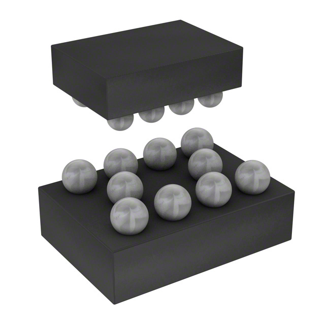
- Part No.:
- PCMF2USB3S/CZ
- Manufacturer:
- Nexperia USA Inc.
- Category:
- Common Mode Chokes
- Package:
- 10-UFBGA, WLCSP
- Datasheet:
-
 PCMF2USB3S/CZ.pdf
- Description:
- CMC 4LN SMD ESD
- Quantity:
- Payment:

- Shipping:

Inventory:7,374
Please send an inquiry. Send us your inquiry, and we will respond immediately.
Product details
Overview
PCMF2USB3S from Nexperia is a dual-channel common-mode EMI filter with integrated ESD protection for high-speed differential interfaces. It provides ±15 kV IEC 61000-4-2 contact ESD protection per line, <0.3 dB differential insertion loss at 1 MHz, and −38 dB common-mode attenuation at 2.6 GHz, deployed in USB 3.2 and HDMI 2.0 signal paths to suppress noise while preserving signal integrity.
For engineers reviewing the PCMF2USB3S datasheet, PCMF2USB3S pinout, PCMF2USB3S application, or PCMF2USB3S equivalent, key selection criteria include differential channel count (2), WLCSP10 package footprint, ESD clamping voltage (6–9 V breakdown), common-mode rejection bandwidth (up to 2.6 GHz), and compatibility with 10 Gbps data rates in USB 3.2 Gen 2 systems.
Technical Context
The device integrates two independent differential channels, each with coupled inductors for common-mode suppression and bidirectional ESD diodes on both input and output sides. Its architecture enables simultaneous filtering and protection without compromising differential impedance matching or timing skew.
It operates across −40 °C to +125 °C ambient temperature, supports 5 V DC input voltage, and delivers <0.25 pF diode capacitance per line at 1 MHz - critical for maintaining eye opening in 10 Gbps USB 3.2 and HDMI 2.0 applications as verified in test board eye diagrams.
Key Specifications
| Parameter | Value and Actual Design Meaning |
|---|---|
| Channels | 2 independent differential channels with dedicated ground terminals (GND_CH1, GND_CH2) |
| ESD Protection | ±15 kV contact discharge per line (IEC 61000-4-2 Level 4), clamping voltage 6–9 V |
| Differential Insertion Loss | ≤0.3 dB at 1 MHz; ≤18 dB at 5 GHz - preserves signal amplitude up to Gen 2 speeds |
| Common-Mode Attenuation | −12 dB at 800 MHz; −38 dB at 2.6 GHz - suppresses RF noise coupling into system ground |
| Diode Capacitance | 0.25 pF per line at 1 MHz and 2.5 V - minimizes signal distortion in high-frequency serial links |
| Channel Series Resistance | 3 Ω per line (input to output) - limits DC voltage drop and power dissipation in continuous operation |
| Operating Temperature | −40 °C to +125 °C - supports deployment in thermally demanding mobile and embedded PCB environments |
Pinout & Package
PCMF2USB3S uses the WLCSP10 (4-2-4) wafer-level chip-scale package, measuring 1.62 mm × 1.52 mm × 0.60 mm max, with 10 solder bumps arranged in three rows (A/B/C) and four columns. The package supports fine-pitch PCB assembly with 0.4 mm bump pitch and requires 0.1 mm stencil thickness for reliable reflow.
| Pin/Terminal | Circuit Role | Design Meaning |
|---|---|---|
| A1 | CH1_IN+ | External differential input positive for Channel 1 - connects directly to connector-side USB/HDMI TX/RX trace |
| A2 | CH1_IN− | External differential input negative for Channel 1 - maintains matched length and symmetry with A1 |
| A3 | CH2_IN+ | External differential input positive for Channel 2 - isolates second interface (e.g., DSI or second USB lane) |
| A4 | CH2_IN− | External differential input negative for Channel 2 - routed with identical topology to A3 for crosstalk control |
| B1 | GND_CH1 | Isolated ground return for Channel 1 - prevents noise coupling between channels via shared ground impedance |
| B2 | GND_CH2 | Isolated ground return for Channel 2 - enables independent grounding strategy for multi-interface layouts |
| C1 | CH1_OUT+ | Internal differential output positive for Channel 1 - connects to SoC/PHY side with minimal stub length |
| C2 | CH1_OUT− | Internal differential output negative for Channel 1 - maintains controlled 100 Ω differential impedance per TDR plot |
| C3 | CH2_OUT+ | Internal differential output positive for Channel 2 - decoupled from C1/C2 to avoid inter-channel crosstalk |
| C4 | CH2_OUT− | Internal differential output negative for Channel 2 - validated for <−40 dB crosstalk at 5 GHz per Fig. 3 |
Key Features
| Feature | Design Value |
|---|---|
| Dual-channel common-mode filtering | Independent coil-coupled paths for two differential pairs - eliminates need for discrete LC filters per lane |
| ±15 kV ESD protection per line | IEC 61000-4-2 Level 4 compliance without external TVS - reduces BOM count and PCB area vs. discrete diode solutions |
| 0.25 pF diode capacitance | Preserves >90% eye height in 10 Gbps USB 3.2 eye diagrams (Fig. 5 vs. Fig. 6) - avoids signal degradation at Nyquist frequency |
| WLCSP10 package (4-2-4) | 1.62 mm × 1.52 mm footprint - enables placement directly at USB Type-C or HDMI connectors with minimal trace length |
| −38 dB common-mode rejection at 2.6 GHz | Suppresses radiated emissions from high-speed switching noise - meets Class B EMC requirements without added shielding |
Applications
| USB 3.2 Gen 2 Interface | HDMI 2.0 Serial Link |
|---|---|
Use Scenario: Protecting SuperSpeed TX/RX differential pairs in a smartphone USB Type-C port handling 10 Gbps data transfer. IC Role / Device Role / Timing Role: Common-mode EMI filter and ESD protector placed between connector and SoC PHY, preserving differential impedance and minimizing insertion loss. Use Value: Maintains clean 10 Gbps eye diagram (Fig. 5) while suppressing >30 dB of common-mode noise above 1 GHz - enabling pass/fail compliance with USB-IF electrical specs. |
Use Scenario: Filtering TMDS clock and data lanes in a tablet's HDMI 2.0 output driving a 4K display. IC Role / Device Role / Timing Role: Dual-channel ESD+EMI solution applied to all three TMDS data pairs and clock pair, with isolated grounds per channel. Use Value: Improves HDMI 2.0 eye opening at TP1/TP2 (Figs. 9–12) by reducing jitter induced by common-mode noise - extends cable reach and display compatibility. |
| MIPI D-PHY Camera Interface | MIPI M-PHY DSI Display Interface |
Use Scenario: ESD protection and EMI filtering for CSI-2 differential lanes connecting an image sensor to application processor in automotive ADAS camera module. IC Role / Device Role / Timing Role: Front-end protection device mounted adjacent to FPC connector, handling 1.5 Gbps D-PHY HS mode signals. Use Value: Enables robust operation under ±15 kV ESD stress while maintaining <0.3 dB insertion loss - prevents pixel corruption or frame drop during hot-plug events. |
Use Scenario: Signal conditioning for M-PHY Gear 3 (5.8 Gbps) DSI lanes in a foldable smartphone display subsystem. IC Role / Device Role / Timing Role: Dual-channel filter protecting two independent DSI byte lanes, with separate GND_CH1/GND_CH2 to avoid ground bounce coupling. Use Value: Reduces crosstalk-induced jitter (Fig. 3) and improves PWM-TX eye opening (Figs. 13–16) - ensures stable high-resolution panel refresh without visual artifacts. |
Equivalent & Alternatives
The following parts are listed as comparable options for similar dual-channel differential EMI+ESD protection applications.
| Alternative Part | Technical Difference | Application Difference | Selection Advice |
|---|---|---|---|
| TDK MEM2012W121R | Single-channel, 120 Ω common-mode impedance at 100 MHz; no integrated ESD diodes - requires external TVS | Limited to one differential pair; lacks ±15 kV ESD rating - unsuitable for USB/HDMI front-end protection | Select only when discrete ESD protection is already implemented and common-mode filtering is the sole requirement. |
| ON Semiconductor NUF2221MUTAG | Two-channel, 0.5 pF diode capacitance per line; ±12 kV ESD rating; higher insertion loss (>0.8 dB at 1 GHz) | Valid for USB 2.0 (480 Mbps) but fails eye integrity at 5+ Gbps - marginal for HDMI 2.0 or USB 3.2 | Choose only for cost-sensitive USB 2.0 designs where 10 Gbps performance is not required. |
Compared with TDk MEM2012W121R and ON Semi NUF2221MUTAG, PCMF2USB3S uniquely combines dual-channel integration, ±15 kV ESD, sub-0.3 dB insertion loss at 1 GHz, and 0.25 pF capacitance - making it the only qualified solution for 10 Gbps differential interfaces requiring co-located EMI filtering and ESD protection.
Availability
PCMF2USB3S is available at Aetrix Electronics and suitable for USB 3.2 Gen 2 host ports, HDMI 2.0 display outputs, and MIPI D-PHY camera interfaces requiring stable component supply across high-volume mobile and embedded production programs.
Supply support for PCMF2USB3S includes scheduled delivery planning, volume procurement assistance, BOM continuity management, traceable sourcing, and lifecycle availability coordination for OEM customers, industrial embedded developers, connected-device designers, and electronics production programs.
Manufacturer
Nexperia is a global semiconductor expert focused on high-performance, high-reliability standard logic, analog, and ESD protection devices, serving automotive, industrial, and consumer markets with scalable manufacturing and rigorous AEC-Q200 validation.
PCMF2USB3S belongs to the PCMFxUSB3S series - engineered specifically for high-speed differential signaling standards (USB 3.x, HDMI, MIPI) where simultaneous EMI suppression and robust ±15 kV ESD protection must coexist without degrading signal fidelity.
FAQ
What is the maximum data rate supported by PCMF2USB3S?
PCMF2USB3S supports 10 Gbps differential data rates, as validated by USB 3.2 Gen 2 eye diagrams (Fig. 5) showing full compliance with jitter and amplitude specifications. Its 6 GHz differential −3 dB bandwidth and <0.3 dB insertion loss at 1 MHz ensure signal integrity through PCIe Gen 3, USB 3.2, and HDMI 2.0 physical layers.
Can PCMF2USB3S be used for HDMI 2.0 applications?
Yes - PCMF2USB3S is explicitly qualified for HDMI 2.0, with test data (Figs. 9–12) confirming improved eye opening at 148.5 MHz TMDS clock frequency. Its low 0.25 pF capacitance and symmetric layout preserve differential impedance, while −38 dB common-mode rejection suppresses radiated emissions from long cable runs.
How does the WLCSP10 package affect PCB layout?
The WLCSP10 (1.62 mm × 1.52 mm) requires precise solder stencil design (0.1 mm thickness, 0.4 mm bump pitch) and strict impedance-controlled routing. Its compact size allows placement directly at USB Type-C or HDMI connectors, minimizing unprotected trace length - critical for passing IEC 61000-4-2 ESD testing without system-level failures.
Is PCMF2USB3S automotive-qualified?
No - PCMF2USB3S is not automotive-qualified per AEC-Q200. While it operates from −40 °C to +125 °C, it lacks automotive-specific reliability testing (e.g., HTOL, TC, UHAST). For automotive infotainment or ADAS applications, Nexperia's automotive-grade equivalents (e.g., PCMF2USB3S/AH) must be specified instead.
PCMF2USB3S/CZ Specifications
- Product attributes
- Attribute value
- Manufacturer:
- Nexperia USA Inc.
- Package/Case:
- 10-UFBGA, WLCSP
- Filter Type:
- Signal Line
- Number of Lines:
- 4
- Impedance @ Frequency:
- -
- Current Rating (Max):
- -
- DC Resistance (DCR) (Max):
- -
- Voltage Rating - DC:
- 3Ohm (Typ)
- Voltage Rating - AC:
- -
- Operating Temperature:
- -
- Ratings:
- -40°C ~ 85°C
- Approval Agency:
- -
- Features:
- -
- Mounting Type:
- TVS Diode ESD Protection
- Size / Dimension:
- -
- Height (Max):
- -
PCMF2USB3S/CZ FAQ
1.How can I place an order for PCMF2USB3S/CZ through Aetrix?
Please submit a Request for Quotation (RFQ) for PCMF2USB3S/CZ on Aetrix. Our sales agent will provide a competitive quotation and guide you through the order confirmation once you accept the terms.
2.Are the price and stock information for PCMF2USB3S/CZ reliable?
The price and inventory of PCMF2USB3S/CZ are updated periodically and may fluctuate due to market conditions. Stock and pricing data are typically refreshed every 24 hours. Quotation validity for PCMF2USB3S/CZ is usually 5 days.
3.What payment methods are accepted for PCMF2USB3S/CZ?
We accept Wire Transfer, PayPal, Credit Card, Western Union, MoneyGram, and Escrow for PCMF2USB3S/CZ transactions.
Note: Certain payment methods may incur a processing fee.
4.How is shipping managed for PCMF2USB3S/CZ?
PCMF2USB3S/CZ orders can be shipped via leading logistics carriers, including DHL, UPS, FedEx, TNT, or Registered Mail.
Once your PCMF2USB3S/CZ order is processed, you will receive an email with the shipment details and tracking number.
Note: Tracking information may take up to 24 hours to appear. Express delivery typically takes 3–5 business days.
5.How can I obtain technical support or documentation for PCMF2USB3S/CZ?
For technical support, including PCMF2USB3S/CZ datasheets, pinout diagrams, or application guidance, please contact our engineering support team. They can provide detailed documentation and assistance for your PCMF2USB3S/CZ requirements.
6.How does Aetrix verify that PCMF2USB3S/CZ is sourced from the original manufacturer or authorized distributors?
All PCMF2USB3S/CZ products on Aetrix are procured from qualified distributors and authorized channels. Our dedicated quality assurance team conducts strict verification, including traceability checks and, if necessary, third-party testing. This ensures that PCMF2USB3S/CZ meets industry standards.
7.What is the process for return or replacement of PCMF2USB3S/CZ?
All PCMF2USB3S/CZ units undergo pre-shipment inspection (PSI). If there is an issue with PCMF2USB3S/CZ, returns or replacements are accepted under the following conditions:
1.Quantity discrepancies, incorrect items, or visible external defects (such as breakage or corrosion), acknowledged by Aetrix.
2.The issue is reported within 90 days of delivery.
3.The PCMF2USB3S/CZ part is unused and in its original packaging.
Return procedure for PCMF2USB3S/CZ:
1.Submit a request within 90 days.
2.Obtain a Return Material Authorization (RMA) from Aetrix.
PCMF2USB3S/CZ Tags
-4-Lead.jpg)
-
DLM0NSN900HY2D
Murata Electronics
-
DLM0NSM900HY2D
Murata Electronics

-
DLM0QSN900HY2D
Murata Electronics
-
TCM0605M-900-2P-T201
TDK Corporation
-
LCFE121002A900TG
Littelfuse Inc.
-
DLM11SN900HZ2L
Murata Electronics
-
ACM2012H-381-2P-T05
TDK Corporation
-
SRF2012-900YA
Bourns Inc.
-
ACM2012-900-2P-T002
TDK Corporation
-
ACM2012-361-2P-T002
TDK Corporation
-
ACM2012-121-2P-T002
TDK Corporation
-
ACM2012D-900-2P-T00
TDK Corporation
Tech Hub

Jumper cables guide covering safe connection order, red and black clamp placement, final ground connection, cable gauge, length, clamp quality, copper vs CCA cables, jump starter comparison and battery…

LDO regulator guide covering low dropout voltage, power dissipation, thermal design, PSRR, output noise, capacitor stability, adjustable LDO circuits, LDO vs buck converter and datasheet selection chec…

Conditional Access Module guide covering CAM meaning, CI/CI+ interface, smart card authorization, DVB security workflow, TV and set-top box compatibility, internal electronics, ESD protection, connecto…

Guide to electronic component obsolescence covering EOL risk, PCN/PDN notices, last-time buy planning, replacement options, form-fit-function validation, counterfeit risk and BOM lifecycle management.

18650 battery guide covering lithium-ion cell basics, 3.6V/3.7V voltage, 4.2V charging, mAh and Wh capacity, protected cells, chargers, BMS, series-parallel packs, holders, welding and sourcing checks.…

Hall effect sensor guide covering working principle, linear and digital sensors, Arduino circuits, current sensing, speed detection, automotive applications, A3144 examples, signal filtering and datash…

Product Change Notification guide for electronic components, covering PCN meaning, PCN vs PDN/EOL, common change types, risk levels, form-fit-function review, engineering validation, BOM control, LTB/L…

A practical guide to blend door actuators, covering HVAC function, symptoms, location, AC and heater issues, reset and calibration, replacement cost, electrical diagnosis, compatibility checks, and rep…

Engineering guide to Raspberry Pi alternatives, covering chip-level differences, Orange Pi, ROCK, Jetson, Banana Pi, NanoPi, Compute Module, Pico, GPIO, camera, HAT compatibility, and replacement risks…

Engineering guide to dynamic load response testing for high-current buck converters, covering load step setup, slew rate, Vcore undershoot, overshoot, recovery time, probe location, output capacitors a…


