
 My Inquiry
 My Account


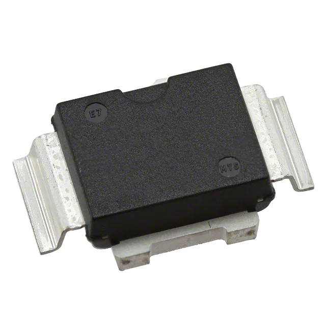
STMicroelectronics PD85035-E
- Part No.:
- PD85035-E
- Manufacturer:
- STMicroelectronics
- Category:
- Single FETs, MOSFETs
- Package:
- PowerSO-10RF Exposed Bottom Pad (2 Formed Leads)
- Datasheet:
-
 PD85035-E.pdf
- Description:
- RF MOSFET LDMOS 13.6V PWRSO-10RF
- Quantity:
- Payment:

- Shipping:

Inventory:6,013
Please send an inquiry. Send us your inquiry, and we will respond immediately.
Product details
Overview
PD85035-E from STMicroelectronics is an N-channel enhancement-mode lateral MOSFET RF power transistor in common-source configuration, rated for 35 W POUT at 870 MHz with 14.9 dB gain and 60–72% drain efficiency at 13.6 V supply. It features 40 V V(BR)DSS, 8 A ID max, 1.0 °C/W RthJC, and ESD protection per HBM Class 2. Designed for car mobile radio amplifiers requiring broadband linearity and thermal stability up to 1 GHz.
For engineers reviewing the PD85035-E datasheet, PD85035-E pinout, PD85035-E application, or PD85035-E equivalent, this page delivers verified electrical specs, PowerSO-10RF package details, thermal performance data, and real-world use cases in mobile RF power stages - all grounded in ST's official Doc ID 13597 Rev 3.
Technical Context
The PD85035-E operates as a single-ended, common-source RF amplifier with fixed gate bias (VGS(Q) = 3.4–4.6 V), optimized for 870 MHz commercial band operation. Its LDMOS structure delivers high transconductance and low output capacitance (COSS = 45 pF), enabling stable broadband matching across 10–1000 MHz.
Thermal design centers on the PowerSO-10RF package's 1.0 °C/W junction-to-case resistance and 165 °C max junction temperature, supporting continuous-wave operation at 35 W with appropriate heatsinking. ESD robustness (HBM Class 2) and moisture sensitivity level MSL 3 ensure manufacturability in standard SMT lines.
Key Specifications
| Parameter | Value and Actual Design Meaning |
|---|---|
| POUT @ 870 MHz | 35 W (P3dB); enables 30–40 W linear output in FM/AM mobile radio final stages |
| Gain @ 870 MHz | 14.9 dB typical; reduces driver stage complexity in two-stage transmitter designs |
| V(BR)DSS | 40 V; supports 13.6 V nominal supply with 3× headroom for voltage transients |
| RthJC | 1.0 °C/W; allows direct mounting to heatsink without thermal interface pad for <100°C rise at 35 W |
| CISS / COSS | 76 pF / 45 pF at 12.5 V; simplifies input/output impedance matching network design |
| Drain Efficiency | 60–72% at P3dB; minimizes DC power draw and heatsink size in battery-backed vehicle systems |
| ESD Rating | HBM Class 2 (2 kV); withstands handling without special ESD controls during assembly |
Pinout & Package
PD85035-E uses the PowerSO-10RF plastic package - ST's first JEDEC-approved high-power SMD RF package - with formed leads (gull wing). The package provides low-inductance source grounding and optimized RF port geometry for minimal parasitic coupling.
| Pin/Terminal | Circuit Role | Design Meaning |
|---|---|---|
| Gate | Control electrode | High-impedance input requiring stable DC bias (3.4–4.6 V) and RF decoupling; sensitive to ESD |
| Source | Common reference node | Low-inductance connection point; internally bonded to exposed metal tab for thermal + RF grounding |
| Drain | RF power output terminal | High-current output node; connected to output matching network and heatsink via metal tab |
Key Features
| Feature | Design Value |
|---|---|
| PowerSO-10RF SMD package | First JEDEC-compliant high-power RF SMD package; eliminates through-hole assembly while maintaining thermal integrity |
| Linearity at P3dB | Supports 20:1 load mismatch tolerance at full power - critical for antenna VSWR variations in mobile radios |
| Thermal stability | 165 °C TJ max + 1.0 °C/W RthJC enables stable gain and efficiency over ambient range (-40 to +85 °C) |
| ESD protection | HBM Class 2 rating ensures compatibility with standard SMT reflow and handling without added protection circuitry |
| Broadband operation | Validated performance from 10 MHz to 1 GHz supports multi-band base station repeaters and trunked radio systems |
Applications
| Car Mobile Radio Amplifier | FM Broadcast Transmitter Stage |
|---|---|
Use Scenario: Final RF power stage in 870 MHz land-mobile radio transceivers for emergency services and fleet communications. IC Role / Device Role / Timing Role: Common-source RF power amplifier delivering 35 W P3dB into 50 Ω load with 14.9 dB small-signal gain. Use Value: High linearity (60–72% efficiency at P3dB) maintains spectral purity under modulation; PowerSO-10RF enables compact PCB layout and automated assembly. |
Use Scenario: Driver or final stage in low-power FM broadcast transmitters (10–30 W ERP) for community radio stations. IC Role / Device Role / Timing Role: Linear RF power amplifier operating at 87.5–108 MHz with broadband impedance matching. Use Value: CISS/COSS values (76 pF/45 pF) simplify broadband matching network design; 40 V V(BR)DSS accommodates 24 V supply rails with margin. |
| Industrial UHF Repeater | Trunked Radio Base Station |
Use Scenario: UHF repeater output stage in industrial automation networks operating at 400–470 MHz. IC Role / Device Role / Timing Role: High-reliability RF power transistor in Class AB configuration with forced-air cooling. Use Value: 1.0 °C/W RthJC enables stable operation at 35 W with passive heatsinking; MSL 3 rating supports standard reflow profiles. |
Use Scenario: Multi-carrier amplifier stage in P25 or TETRA base station equipment requiring wide dynamic range. IC Role / Device Role / Timing Role: Linear RF power device supporting 10–1000 MHz bandwidth with low intermodulation distortion. Use Value: Excellent thermal stability preserves gain flatness across temperature; ESD Class 2 ensures robustness in field-deployed hardware. |
Equivalent & Alternatives
The following parts are listed as comparable options for similar RF power amplifier applications.
| Alternative Part | Technical Difference | Application Difference | Selection Advice |
|---|---|---|---|
| MRF6P20140HR5 | Higher POUT (140 W), GaN-on-SiC, 28 V operation, RthJC = 0.45 °C/W | Requires redesigned DC biasing, matching, and thermal management; not drop-in | Select for >100 W systems where efficiency and bandwidth outweigh cost and complexity |
| PD57003-E | LDMOS, 3 W POUT, same PowerSO-10RF package, 28 V V(BR)DSS, lower gain (12.5 dB) | Lower power tier; suitable for driver stages but not final amplification | Choose when scaling down to sub-10 W output with identical footprint and thermal behavior |
Compared with MRF6P20140HR5 and PD57003-E, PD85035-E uniquely balances 35 W output, 13.6 V compatibility, and PowerSO-10RF manufacturability - making it optimal for cost-sensitive, thermally constrained mobile radio final stages.
Availability
PD85035-E is available at Aetrix Electronics and suitable for car mobile radio amplifiers, FM broadcast transmitters, and industrial UHF repeaters requiring stable component supply, JEDEC-compliant SMD packaging, and proven RF linearity at 870 MHz.
Supply support for PD85035-E includes scheduled delivery planning, volume procurement assistance, BOM continuity management, traceable sourcing, and lifecycle availability coordination for OEM customers, industrial embedded developers, connected-device designers, and electronics production programs.
Manufacturer
STMicroelectronics is a global semiconductor leader headquartered in Geneva, Switzerland, designing and manufacturing microcontrollers, power devices, sensors, and analog ICs for automotive, industrial, and consumer markets.
PD85035-E belongs to ST's LdmoST plastic family of RF power transistors - engineered specifically for high-efficiency, broadband mobile and industrial radio amplifiers operating below 1 GHz.
FAQ
What is the recommended gate bias voltage for PD85035-E in Class AB operation?
The datasheet specifies VGS(Q) = 3.4–4.6 V at ID = 250 mA and VDS = 10 V. For stable Class AB operation at IDQ = 350 mA, a gate bias of 4.2 V ±0.2 V is recommended, verified by Figure 7 and Table 4. This setting achieves optimal gain-efficiency trade-off at 870 MHz with 13.6 V supply.
Can PD85035-E be used at frequencies above 1 GHz?
No - the device is characterized and guaranteed only up to 1 GHz. Gain drops sharply beyond 950 MHz (Figure 9 shows <10 dB at 1 GHz), and load mismatch tolerance degrades. ST explicitly rates it for "up to 1 GHz" in the description, and no performance data is provided above that frequency.
Is the PowerSO-10RF package lead-free and RoHS compliant?
Yes - PD85035-E is offered in ECOPACK®-compliant versions. ST's documentation confirms compliance with Directive 2002/95/EC (RoHS), and the PowerSO-10RF package uses lead-free terminations. MSL 3 rating (per J-STD-020B) further confirms suitability for Pb-free reflow processes.
Does PD85035-E require external ESD protection in the circuit?
No - the device integrates on-chip ESD protection rated to HBM Class 2 (2 kV), as confirmed in Table 6. No external TVS diodes or series resistors are required for handling or board-level ESD immunity, though good RF layout practices (grounding, decoupling) remain essential for signal integrity.
PD85035-E Specifications
- Product attributes
- Attribute value
- Manufacturer:
- STMicroelectronics
- Series:
- -
- Package/Case:
- PowerSO-10RF Exposed Bottom Pad (2 Formed Leads)
- Packaging:
- Tube
- Product Status:
- Active
- Technology:
- LDMOS
- Configuration:
- -
- Frequency:
- 870MHz
- Gain:
- 17dB
- Voltage - Test:
- 13.6 V
- Current Rating (Amps):
- 8A
- Noise Figure:
- -
- Current - Test:
- 350 mA
- Power - Output:
- 15W
- Voltage - Rated:
- 40 V
- Grade:
- -
- Qualification:
- -
- Mounting Type:
- -
- Supplier Device Package:
- PowerSO-10RF (Formed Lead)
PD85035-E FAQ
1.How can I place an order for PD85035-E through Aetrix?
Please submit a Request for Quotation (RFQ) for PD85035-E on Aetrix. Our sales agent will provide a competitive quotation and guide you through the order confirmation once you accept the terms.
2.Are the price and stock information for PD85035-E reliable?
The price and inventory of PD85035-E are updated periodically and may fluctuate due to market conditions. Stock and pricing data are typically refreshed every 24 hours. Quotation validity for PD85035-E is usually 5 days.
3.What payment methods are accepted for PD85035-E?
We accept Wire Transfer, PayPal, Credit Card, Western Union, MoneyGram, and Escrow for PD85035-E transactions.
Note: Certain payment methods may incur a processing fee.
4.How is shipping managed for PD85035-E?
PD85035-E orders can be shipped via leading logistics carriers, including DHL, UPS, FedEx, TNT, or Registered Mail.
Once your PD85035-E order is processed, you will receive an email with the shipment details and tracking number.
Note: Tracking information may take up to 24 hours to appear. Express delivery typically takes 3–5 business days.
5.How can I obtain technical support or documentation for PD85035-E?
For technical support, including PD85035-E datasheets, pinout diagrams, or application guidance, please contact our engineering support team. They can provide detailed documentation and assistance for your PD85035-E requirements.
6.How does Aetrix verify that PD85035-E is sourced from the original manufacturer or authorized distributors?
All PD85035-E products on Aetrix are procured from qualified distributors and authorized channels. Our dedicated quality assurance team conducts strict verification, including traceability checks and, if necessary, third-party testing. This ensures that PD85035-E meets industry standards.
7.What is the process for return or replacement of PD85035-E?
All PD85035-E units undergo pre-shipment inspection (PSI). If there is an issue with PD85035-E, returns or replacements are accepted under the following conditions:
1.Quantity discrepancies, incorrect items, or visible external defects (such as breakage or corrosion), acknowledged by Aetrix.
2.The issue is reported within 90 days of delivery.
3.The PD85035-E part is unused and in its original packaging.
Return procedure for PD85035-E:
1.Submit a request within 90 days.
2.Obtain a Return Material Authorization (RMA) from Aetrix.
PD85035-E Tags
-
3SK294(TE85L,F)
Toshiba Semiconductor and Storage

-
SAV-551+
Mini-Circuits

-
TAV2-501+
Mini-Circuits
-
CE3514M4-C2
CEL
-
AFT05MS004NT1
NXP USA Inc.
-
SAV-541+
Mini-Circuits
-
CE3512K2-C1
CEL
-
AFM907NT1
NXP Semiconductors
-
SKY65050-372LF
Skyworks Solutions Inc.
-
CE3520K3-C1
CEL
-
AFT09MS007NT1
NXP USA Inc.
-
AFT09MS015NT1
NXP USA Inc.
Tech Hub

A practical engineering and sourcing framework covering lifecycle verification, lifetime-buy calculations, replacement qualification, supplier checks and counterfeit-risk controls.

TTL and CMOS logic families differ in thresholds, loading, output drive, power and timing. This engineering guide compares 74HC and 74HCT, calculates noise margins and checks 3.3 V/5 V compatibility.

A practical engineering guide to 3.3V and 5V logic compatibility, input thresholds, resistor dividers, translator ICs, MOSFET level shifting, I2C pull-ups, timing limits and power-sequencing risks.

The 74HC595 uses push-pull logic outputs, while the TPIC6B595 uses 50 V open-drain DMOS sinks for higher-power loads. This guide compares timing, current limits, 3.3 V interfacing, load wiring, thermal…

The 74HC595 converts serial data into eight stable parallel outputs. This guide covers pin functions, shift and storage timing, OE and MR behavior, drive-current limits, cascading, voltage compatibilit…

A technical comparison of level-sensitive latches and edge-triggered flip-flops, covering timing windows, setup and hold limits, master–slave operation, time borrowing, race-through, HDL inference and…

A D latch stores one bit while Enable controls when data can pass. This reference covers gate-level operation, truth tables, transparency, setup and hold timing, LE versus OE, common ICs and practical …

An SR latch stores one bit through cross-coupled feedback. This engineering reference covers NOR and NAND implementations, truth tables, forbidden-state recovery, gated operation, switch debouncing, fa…

Latch circuits retain one bit through feedback. This technical reference covers SR and D latches, truth tables, transparency, timing limits, latch-versus-flip-flop behavior, applications and common log…

An engineering guide to LED driver operation, constant-current and constant-voltage outputs, linear and switching topologies, dimming, IC selection, calculations, replacement compatibility, and fault c…


