
 My Inquiry
 My Account


Nexperia USA Inc. PDTB143XTR
- Part No.:
- PDTB143XTR
- Manufacturer:
- Nexperia USA Inc.
- Category:
- Single, Pre-Biased Bipolar Transistors
- Package:
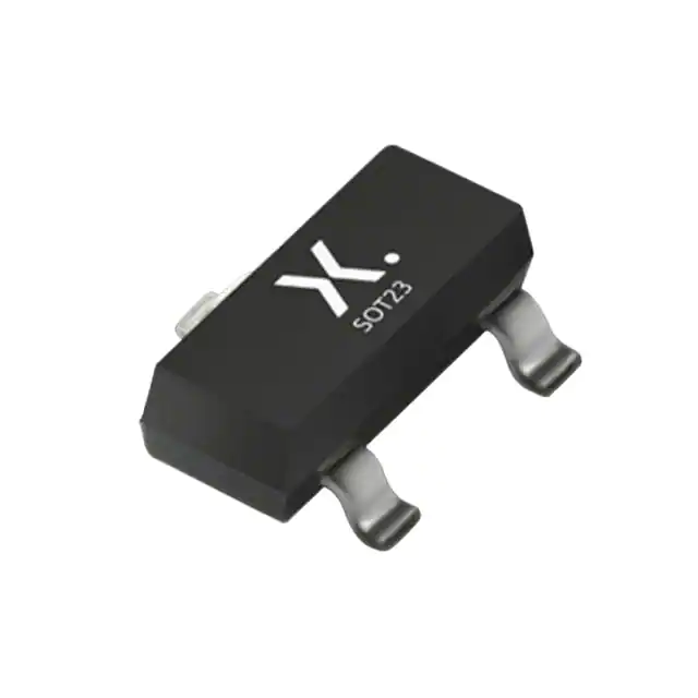
- TO-236-3, SC-59, SOT-23-3
- Datasheet:
-
 PDTB143XTR.pdf
- Description:
- TRANS PREBIAS PNP 50V TO236AB
- Quantity:
- Payment:

- Shipping:

Inventory:396
Please send an inquiry. Send us your inquiry, and we will respond immediately.
Product details
Overview
PDTB143XTR from Nexperia is a PNP resistor-equipped transistor (RET) in SOT23 (TO-236AB) package, designed for digital switching applications with built-in bias resistors R1 = 4.7 kΩ and R2 = 10 kΩ, −50 V VCEO, −500 mA IO, and AEC-Q101 qualification for automotive use.
For engineers reviewing the PDTB143XTR datasheet, PDTB143XTR pinout, PDTB143XTR application, or PDTB143XTR equivalent, key selection factors include its integrated 4.7 kΩ/10 kΩ resistor ratio (R2/R1 ≈ 2.13), −1.4 V typical VI(on) at −20 mA, −100 mV VCE(sat) at −50 mA/−2.5 mA, and operation up to +175 °C ambient.
Technical Context
This PNP RET integrates two precision bias resistors (R1 = 4.7 kΩ input resistor, R2 = 10 kΩ base-emitter resistor) to eliminate external components for digital logic interfacing. Its R2/R1 ratio of 2.13 enables stable current gain control and reduces sensitivity to transistor hFE variation.
The device operates as a single-stage saturated switch with guaranteed −500 mA output capability and low −100 mV saturation voltage under −50 mA collector current and −2.5 mA base drive, supporting high-efficiency load control in space-constrained PCB layouts.
Key Specifications
| Parameter | Value and Actual Design Meaning |
|---|---|
| VCEO | −50 V - Maximum safe collector-emitter voltage before breakdown; supports 24 V and 48 V industrial bus switching. |
| IO | −500 mA - Continuous DC output current rating; suitable for driving relays, LEDs, and small solenoids. |
| R1 / R2 | 4.7 kΩ / 10 kΩ - Fixed internal bias network eliminates need for external resistors; simplifies layout and improves BOM consistency. |
| VCE(sat) | −100 mV @ IC = −50 mA, IB = −2.5 mA - Low conduction loss enables high efficiency in battery-powered and thermally constrained systems. |
| Tj(max) | +175 °C - Junction temperature limit enabling deployment in under-hood automotive and high-temperature industrial environments. |
| AEC-Q101 | Qualified - Meets stress test requirements for discrete semiconductors in automotive applications; supports ASIL-B system integration. |
| hFE | 70 @ VCE = −5 V, IC = −50 mA - Guaranteed DC current gain ensures reliable turn-on margin across process and temperature variations. |
Pinout & Package
SOT23 (TO-236AB) plastic surface-mounted package: 3-pin, 1.3 mm × 2.9 mm footprint, 1.1 mm height, optimized for reflow and wave soldering per IPC-7351 standards.
| Pin/Terminal | Circuit Role | Design Meaning |
|---|---|---|
| 1 | Input (base) | Connected internally to R1; accepts logic-level drive (e.g., 3.3 V or 5 V MCU GPIO) without external current-limiting resistor. |
| 2 | GND (emitter) | Common reference node; ties emitter to ground plane; serves as return path for both input and output currents. |
| 3 | Output (collector) | Switched high-side load connection point; sinks up to −500 mA when pin 1 is driven low relative to pin 2. |
Key Features
| Feature | Design Value |
|---|---|
| Integrated bias network | Eliminates two external resistors, reducing PCB area by ≥2.5 mm² and improving assembly yield in automated SMT lines. |
| ±10 % resistor ratio tolerance | Ensures consistent switching thresholds across production lots, minimizing calibration effort in volume manufacturing. |
| High-temperature operation | Rated for continuous operation from −55 °C to +175 °C ambient, supporting engine control units and powertrain modules. |
| Low VI(off) | −0.75 V typical off-state input voltage enables reliable cutoff with TTL/CMOS-compatible logic families. |
| Cost-saving alternative | Direct functional replacement for BC807/BC817 in digital switching roles, reducing total system cost without redesign. |
Applications
| Automotive Body Control Module | Industrial PLC Output Stage |
|---|---|
Use Scenario: Controlling door lock actuators and interior lighting via microcontroller GPIO. IC Role / Device Role / Timing Role: PNP RET acts as a grounded-emitter load switch, sinking current from 12 V loads to MCU-controlled ground. Use Value: Built-in resistors enable direct 3.3 V GPIO drive; AEC-Q101 qualification ensures reliability over 15-year vehicle lifetime. | Use Scenario: Driving 24 V DC solenoid valves in factory automation I/O modules. IC Role / Device Role / Timing Role: High-current digital switch interfacing between isolated logic and inductive loads. Use Value: −500 mA rating and −100 mV VCE(sat) minimize heat generation in densely packed DIN-rail enclosures. |
| Consumer Appliance Power Sequencing | Medical Diagnostic Equipment Fan Control |
Use Scenario: Enabling/disabling auxiliary power rails during startup and fault recovery in smart washing machines. IC Role / Device Role / Timing Role: Logic-level controlled power gate managing sequencing timing between main and auxiliary supplies. Use Value: −1.4 V typical VI(on) ensures compatibility with low-voltage MCUs; ±10 % resistor tolerance maintains timing accuracy across batches. | Use Scenario: Regulating cooling fan speed in portable ultrasound devices using PWM-driven switching. IC Role / Device Role / Timing Role: Fast-switching PNP driver converting MCU PWM signals into high-current fan drive. Use Value: 140 MHz fT supports clean PWM edges up to 20 kHz; 175 °C Tj(max) accommodates sealed thermal enclosures. |
Equivalent & Alternatives
The following parts are listed as comparable options for similar PNP resistor-equipped transistor applications.
| Alternative Part | Technical Difference | Application Difference | Selection Advice |
|---|---|---|---|
| PDTB143ET | R2 = 4.7 kΩ (R2/R1 = 1.0); lower VI(off) (−0.9 V typ); higher hFE variation tolerance | Better suited for general-purpose logic interfacing where precise threshold control is less critical | Select when matching legacy BC807-40 behavior or requiring tighter VI(off) spec |
| PDTC143XT | NPN complement; same R1/R2 values; requires inverted logic drive and high-side supply configuration | Used where load must be connected to VCC rather than ground (e.g., high-side LED drivers) | Select only when circuit topology mandates NPN sourcing instead of PNP sinking |
Compared with PDTB143ET, PDTB143XTR offers higher R2/R1 ratio (2.13 vs. 1.0) for improved noise immunity and more predictable turn-off; versus PDTC143XT, it provides native low-side switching without level-shifting, reducing component count in MCU-peripheral interfaces.
Availability
PDTB143XTR is available at Aetrix Electronics and suitable for automotive body electronics, industrial PLC outputs, consumer appliance power sequencing, and medical diagnostic equipment requiring stable component supply and AEC-Q101 compliance.
Supply support for PDTB143XTR includes scheduled delivery planning, volume procurement assistance, BOM continuity management, traceable sourcing, and lifecycle availability coordination for OEM customers, industrial embedded developers, connected-device designers, and electronics production programs.
Manufacturer
Nexperia is a global semiconductor expert delivering high-performance, reliable discrete, logic, and MOSFET devices with focus on efficiency, miniaturization, and automotive-grade quality.
The PDTB1xxxT series targets cost-sensitive, high-volume digital switching applications where integrated biasing, AEC-Q101 qualification, and SOT23 scalability are essential design requirements.
FAQ
What is the maximum continuous collector current for PDTB143XTR?
The PDTB143XTR is rated for −500 mA continuous DC output current under standard PCB mounting conditions (FR4, single-sided copper). Derating applies above +25 °C ambient per the 470 K/W junction-to-ambient thermal resistance; at +100 °C ambient, maximum usable current drops to approximately −320 mA to maintain Tj ≤ +175 °C.
Does PDTB143XTR require an external base resistor when driven by a 3.3 V MCU GPIO?
No external base resistor is required. The integrated R1 = 4.7 kΩ input resistor limits base current to ~0.5 mA when driven from 3.3 V, providing sufficient drive for −50 mA collector current while maintaining saturation. This eliminates one passive component and associated layout area in digital interface designs.
How does the R2/R1 ratio of 2.13 affect switching performance?
The R2/R1 ratio of 2.13 sets the internal feedback bias that stabilizes operating point against hFE variation and temperature drift. It results in a typical VI(on) of −1.4 V and VI(off) of −0.75 V, enabling robust noise margins (>0.6 V) in noisy automotive and industrial environments without additional hysteresis circuitry.
Can PDTB143XTR replace BC807-40 in existing designs?
Yes - PDTB143XTR is a drop-in functional replacement for BC807-40 in digital switching applications. It matches the SOT23 pinout (pin 1 = base, pin 2 = emitter, pin 3 = collector), provides superior thermal performance (+175 °C vs. +150 °C), and eliminates two external resistors. Layout changes are unnecessary; only firmware logic polarity may require verification due to PNP vs. NPN topology.
PDTB143XTR Specifications
- Product attributes
- Attribute value
- Manufacturer:
- Nexperia USA Inc.
- Series:
- -
- Package/Case:
- TO-236-3, SC-59, SOT-23-3
- Packaging:
- Tape & Reel (TR)
- Product Status:
- Active
- Transistor Type:
- PNP - Pre-Biased
- Current - Collector (Ic) (Max):
- 500 mA
- Voltage - Collector Emitter Breakdown (Max):
- 50 V
- Resistor - Base (R1):
- 4.7 kOhms
- Resistor - Emitter Base (R2):
- 10 kOhms
- DC Current Gain (hFE) (Min) @ Ic, Vce:
- 70 @ 50mA, 5V
- Vce Saturation (Max) @ Ib, Ic:
- 100mV @ 2.5mA, 50mA
- Current - Collector Cutoff (Max):
- 500nA
- Frequency - Transition:
- 140 MHz
- Power - Max:
- 320 mW
- Grade:
- Automotive
- Qualification:
- AEC-Q100
- Mounting Type:
- Surface Mount
- Supplier Device Package:
- TO-236AB
PDTB143XTR FAQ
1.How can I place an order for PDTB143XTR through Aetrix?
Please submit a Request for Quotation (RFQ) for PDTB143XTR on Aetrix. Our sales agent will provide a competitive quotation and guide you through the order confirmation once you accept the terms.
2.Are the price and stock information for PDTB143XTR reliable?
The price and inventory of PDTB143XTR are updated periodically and may fluctuate due to market conditions. Stock and pricing data are typically refreshed every 24 hours. Quotation validity for PDTB143XTR is usually 5 days.
3.What payment methods are accepted for PDTB143XTR?
We accept Wire Transfer, PayPal, Credit Card, Western Union, MoneyGram, and Escrow for PDTB143XTR transactions.
Note: Certain payment methods may incur a processing fee.
4.How is shipping managed for PDTB143XTR?
PDTB143XTR orders can be shipped via leading logistics carriers, including DHL, UPS, FedEx, TNT, or Registered Mail.
Once your PDTB143XTR order is processed, you will receive an email with the shipment details and tracking number.
Note: Tracking information may take up to 24 hours to appear. Express delivery typically takes 3–5 business days.
5.How can I obtain technical support or documentation for PDTB143XTR?
For technical support, including PDTB143XTR datasheets, pinout diagrams, or application guidance, please contact our engineering support team. They can provide detailed documentation and assistance for your PDTB143XTR requirements.
6.How does Aetrix verify that PDTB143XTR is sourced from the original manufacturer or authorized distributors?
All PDTB143XTR products on Aetrix are procured from qualified distributors and authorized channels. Our dedicated quality assurance team conducts strict verification, including traceability checks and, if necessary, third-party testing. This ensures that PDTB143XTR meets industry standards.
7.What is the process for return or replacement of PDTB143XTR?
All PDTB143XTR units undergo pre-shipment inspection (PSI). If there is an issue with PDTB143XTR, returns or replacements are accepted under the following conditions:
1.Quantity discrepancies, incorrect items, or visible external defects (such as breakage or corrosion), acknowledged by Aetrix.
2.The issue is reported within 90 days of delivery.
3.The PDTB143XTR part is unused and in its original packaging.
Return procedure for PDTB143XTR:
1.Submit a request within 90 days.
2.Obtain a Return Material Authorization (RMA) from Aetrix.
PDTB143XTR Tags
-
MUN5211T1G
onsemi
-
DTC043ZEBTL
Rohm Semiconductor
-
DTC114EKAT146
Rohm Semiconductor
-
DDTD113ZC-7-F
Diodes Incorporated
-
DRDNB16W-7
Diodes Incorporated
-
PDTC114ET,215
Nexperia USA Inc.
-
PDTC143ZT,215
Nexperia USA Inc.
-
PDTC143ET,215
Nexperia USA Inc.
-
PDTC143XT,215
Nexperia USA Inc.
-
MMUN2211LT1G
onsemi
-
PDTC144ET,215
Nexperia USA Inc.
-
PDTC124ET,215
Nexperia USA Inc.
Tech Hub

Operational amplifier guide covering op amp basics, feedback, ideal vs real op amps, common configurations, buffer circuits, offset, bias current, gain-bandwidth, slew rate, rail-to-rail limits and sel…

Jumper cables guide covering safe connection order, red and black clamp placement, final ground connection, cable gauge, length, clamp quality, copper vs CCA cables, jump starter comparison and battery…

LDO regulator guide covering low dropout voltage, power dissipation, thermal design, PSRR, output noise, capacitor stability, adjustable LDO circuits, LDO vs buck converter and datasheet selection chec…

Conditional Access Module guide covering CAM meaning, CI/CI+ interface, smart card authorization, DVB security workflow, TV and set-top box compatibility, internal electronics, ESD protection, connecto…

Guide to electronic component obsolescence covering EOL risk, PCN/PDN notices, last-time buy planning, replacement options, form-fit-function validation, counterfeit risk and BOM lifecycle management.

18650 battery guide covering lithium-ion cell basics, 3.6V/3.7V voltage, 4.2V charging, mAh and Wh capacity, protected cells, chargers, BMS, series-parallel packs, holders, welding and sourcing checks.…

Hall effect sensor guide covering working principle, linear and digital sensors, Arduino circuits, current sensing, speed detection, automotive applications, A3144 examples, signal filtering and datash…

Product Change Notification guide for electronic components, covering PCN meaning, PCN vs PDN/EOL, common change types, risk levels, form-fit-function review, engineering validation, BOM control, LTB/L…

A practical guide to blend door actuators, covering HVAC function, symptoms, location, AC and heater issues, reset and calibration, replacement cost, electrical diagnosis, compatibility checks, and rep…

Engineering guide to Raspberry Pi alternatives, covering chip-level differences, Orange Pi, ROCK, Jetson, Banana Pi, NanoPi, Compute Module, Pico, GPIO, camera, HAT compatibility, and replacement risks…


