
 My Inquiry
 My Account


Infineon Technologies PEB2047-1BNMTSL
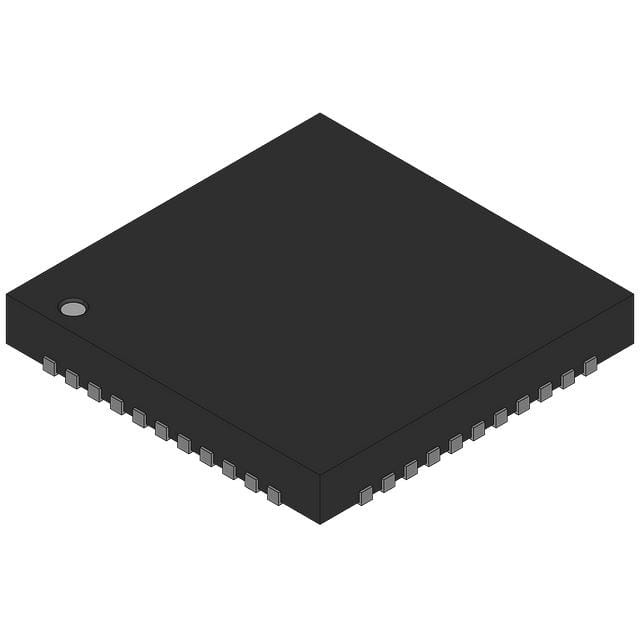
- Part No.:
- PEB2047-1BNMTSL
- Manufacturer:
- Infineon Technologies
- Category:
- Specialized ICs
- Package:
- 44-LCC (J-Lead)
- Datasheet:
-
 PEB2047-1BNMTSL.pdf
- Description:
- IC MEMORY 44PLCC
- Quantity:
- Payment:

- Shipping:

Inventory:456
Please send an inquiry. Send us your inquiry, and we will respond immediately.
Product details
Overview
PEB2047-1BNMTSL from Siemens AG is a non-blocking CMOS memory time switch large (MTSL) IC for PCM telecommunication systems, supporting 4096-, 8192-, or 16384-kHz device clocks, 16 input/8 output PCM lines, and up to 1024×1024 channel switching with per-time-slot programmable constant or minimal delay. It integrates µP interface (8-bit Motorola/Intel), built-in self-test, and tristate output capability for tandem expansion.
For engineers reviewing the PEB2047-1BNMTSL datasheet, PEB2047-1BNMTSL pinout, PEB2047-1BNMTSL application, or PEB2047-1BNMTSL equivalent, key selection criteria include frame-synchronized PCM switching latency control, dual-bus interface mode configuration (multiplexed/demultiplexed), open-drain interrupt signaling, and per-input line delay measurement capability in telecom timing-critical infrastructure.
Technical Context
The PEB2047-1BNMTSL implements a time-division multiplexing (TDM) switch fabric with internal RAM-based time-slot interconnection mapping, enabling non-blocking routing between 16 serial PCM inputs and 8 outputs. Its clock shift mechanism supports half-clock-step resolution for both input and output paths, and each of the 8 primary PCM inputs (IN0–IN7) features individual line delay measurement.
Frame synchronization is achieved via dedicated FSx pins (IN8–IN15) used as frame evaluation inputs, while the SP pin provides system-level synchronization pulse alignment. The device operates exclusively from a single 5 V ±5 % supply and supports two µP interface modes-Motorola (RD/WR/DS) and Intel (ALE/RD/WR)-selected via internal register configuration.
Key Specifications
| Parameter | Value and Actual Design Meaning |
|---|---|
| Switch Capacity | 1024×1024 PCM channels - enables full crosspoint routing in E1/T1 trunk interfaces without blocking. |
| PCM Interface | 16 input / 8 output lines - supports dual E1 (32 time slots × 2) or quad T1 (24 time slots × 4) aggregation. |
| Device Clock | 4096 / 8192 / 16384 kHz - selectable frequency aligns with standard PCM bit rates (2.048/4.096/8.192 Mbps). |
| µP Interface | 8-bit Motorola or Intel bus - flexible host controller integration with configurable address/data multiplexing. |
| Supply Voltage | 5 V ±5 % - single-rail operation simplifies power design in legacy telecom line cards. |
| Interrupt Output | Open-drain INT (Pin 6) - allows wired-OR interrupt sharing across multiple MTSL devices in multi-chip switch fabrics. |
| Delay Control | Per-time-slot constant/minimal delay programming - ensures deterministic jitter performance in voice-grade transmission. |
Pinout & Package
Packaged in P-LCC-44 (SMD), the PEB2047-1BNMTSL uses a 44-pin leadless chip carrier with exposed thermal pad, optimized for high-density telecom PCB layouts and reflow soldering.
| Pin/Terminal | Circuit Role | Design Meaning |
|---|---|---|
| 1 | VSS | Ground reference for all digital and analog circuitry; must be low-impedance connection to minimize switching noise. |
| 3 | SP | Synchronization Pulse input - aligns internal frame counters to external PCM system timing reference. |
| 4–13, 15–17 | IN0–IN7, IN8/FS0–IN15/FS7 | 16 serial PCM input ports - first 8 are data-only; next 8 double as frame sync evaluation inputs for multi-frame alignment. |
| 21–22, 26–34 | A0/A1, AD0–AD7 | Address/data bus interface - supports multiplexed (Intel/Motorola) or demultiplexed microprocessor access to internal registers. |
| 23 | VDD | 5 V power supply - requires local 100 nF + 10 µF decoupling near pin to suppress high-frequency current transients. |
| 24–25, 39 | RD/DS, WR/R/W, RES | Control signals - define read/write cycle timing and reset state initialization for safe boot and error recovery. |
| 35–43 | OUT0–OUT7 | 8 tristatable PCM output ports - enable cascading or shared bus architectures without external bus buffers. |
| 44 | CLK | Master device clock input - determines fundamental PCM bit rate and internal timing granularity. |
| 6 | INT (OD) | Open-drain interrupt output - asserts low on status events (e.g., frame error, register access completion) for host polling reduction. |
Key Features
| Feature | Design Value |
|---|---|
| Non-blocking switch fabric | Guarantees lossless time-slot routing under full load, critical for mission-critical voice trunking where packet loss is unacceptable. |
| Per-input line delay measurement | Enables real-time skew compensation across 8 PCM inputs, ensuring frame-aligned output in distributed timing environments. |
| Half-clock-step clock shift | Provides 122 ns (at 8.192 MHz) fine-grained phase adjustment for input/output paths, reducing intersymbol interference in long-haul links. |
| Built-in self-test (BIST) | Verifies internal RAM and logic integrity at power-up or on-demand, eliminating need for external test vectors in field-deployed systems. |
| Tristate output capability | Allows direct connection of multiple MTSL outputs to shared backplane buses, simplifying modular switch fabric scaling. |
Applications
| PCM Multiplexer/Demultiplexer | E1/T1 Line Card Aggregation |
|---|---|
Use Scenario: Consolidating 16 E1 streams (2.048 Mbps each) into a single high-speed backplane interface for central office switching. IC Role / Device Role / Timing Role: Time-slot interchanger performing synchronous TDM grooming with deterministic delay per slot. Use Value: Enables precise alignment of 32 time slots per E1 frame across all 16 inputs, preserving voice payload integrity without buffer-induced jitter. | Use Scenario: Building modular T1 line cards supporting up to 96 DS0 channels in carrier-class access equipment. IC Role / Device Role / Timing Role: Central time-switching engine managing channelized T1 framing and cross-connect provisioning. Use Value: Supports per-channel delay programming to meet GR-474-CORE jitter compliance for Class 3 timing in SONET/SDH edge nodes. |
| Digital Cross-Connect System (DCS) | PCM-Based Voice Gateway |
Use Scenario: Implementing a 1024×1024 non-blocking digital cross-connect for legacy PSTN interconnection points. IC Role / Device Role / Timing Role: Core switching matrix handling bidirectional PCM traffic with independent input/output clock domains. Use Value: Delivers sub-microsecond path delay consistency across all 1024 channels, meeting ITU-T G.823 wander tolerance requirements. | Use Scenario: Bridging analog voice lines to VoIP gateways using TDM-over-IP encapsulation. IC Role / Device Role / Timing Role: Synchronizing legacy PCM timing to packetized media streams via precise frame boundary detection. Use Value: Uses FSx pins to detect and lock onto incoming E1 frame alignment, enabling seamless clock recovery for RTP timestamp generation. |
Equivalent & Alternatives
The following parts are listed as comparable options for similar time-slot switching applications.
| Alternative Part | Technical Difference | Application Difference | Selection Advice |
|---|---|---|---|
| PEF2047-N-16 | Same die, different ordering code; identical electrical specs and pinout; manufactured under same Q67100-H6301 package spec. | No functional difference - used interchangeably in Siemens' own system designs and reference schematics. | Select when sourcing from legacy Siemens distribution channels or when matching existing BOMs referencing PEF prefix. |
| MT8985D from Mitel | Supports only 2048-kHz base clock; lacks per-input line delay measurement; uses 5 V CMOS but no open-drain INT. | Limited to smaller-scale E1 concentrators (<512 channels); unsuitable for multi-frame alignment or jitter-sensitive DCS deployments. | Choose only for cost-sensitive, lower-port-count applications where half-clock-step adjustment and FSx evaluation are not required. |
Compared with PEF2047-N-16 (identical functionality) and MT8985D (reduced feature set), the PEB2047-1BNMTSL uniquely delivers 16384-kHz operation, per-input delay calibration, and open-drain interrupt support - essential for scalable, jitter-controlled telecom infrastructure.
Availability
PEB2047-1BNMTSL is available at Aetrix Electronics and suitable for E1/T1 line card development, digital cross-connect systems, PCM multiplexers, and voice gateway hardware requiring stable component supply and long-term obsolescence management.
Supply support for PEB2047-1BNMTSL includes scheduled delivery planning, volume procurement assistance, BOM continuity management, traceable sourcing, and lifecycle availability coordination for OEM customers, industrial embedded developers, connected-device designers, and electronics production programs.
Manufacturer
Siemens AG Semiconductor Group (now Infineon Technologies) was a leading European semiconductor manufacturer specializing in industrial, automotive, and telecommunications ICs before spinning off its chip business in 1999.
The MTSL product line-including PEB2047-was engineered specifically for time-critical PCM switching in public switched telephone network (PSTN) infrastructure, emphasizing deterministic delay, frame synchronization fidelity, and multi-chip scalability.
FAQ
What µP interface modes does PEB2047-1BNMTSL support?
The device supports both Motorola-style (RD/WR/DS) and Intel-style (ALE/RD/WR) 8-bit parallel microprocessor interfaces. Mode selection is configured via internal registers during initialization; pin ALE must be tied to VDD for Motorola mode or driven actively for Intel mode. No external mode-select pins are required.
How is frame synchronization implemented on PEB2047-1BNMTSL?
Frame sync is handled through dedicated FSx pins (IN8–IN15), which double as PCM inputs and frame evaluation inputs. The STAR register's FSAD[2:1] bits configure which FS input pair defines the frame alignment window. Internal logic measures arrival skew relative to SP and adjusts clock shift accordingly to maintain zero-jitter output framing.
Does PEB2047-1BNMTSL support hot-swap or dynamic reconfiguration?
No dynamic reconfiguration is supported during active switching. Register writes require the device to be in idle state (no ongoing frame transfers). However, the RES pin allows full hardware reset without power cycling, and the tristate outputs prevent bus contention during initialization-enabling controlled firmware updates in redundant line card architectures.
What is the significance of the "-16" suffix in PEB2047-1BNMTSL?
The "-16" denotes full support for 16384-kHz device clock operation and associated features-including extended frame delay measurement range and enhanced clock shift resolution-unavailable in earlier PEB2047 variants. This version also includes updated mask ROM with Revision 2.1 firmware and corrected timing parameters per Edition 03.95 datasheet.
PEB2047-1BNMTSL Specifications
- Product attributes
- Attribute value
- Manufacturer:
- Infineon Technologies
- Series:
- -
- Package/Case:
- 44-LCC (J-Lead)
- Packaging:
- Bulk
- Product Status:
- Active
- Programmable:
- Not Verified
- Type:
- Memory
- Applications:
- -
- Mounting Type:
- Surface Mount
- Supplier Device Package:
- 44-PLCC (16.6x16.6)
- Grade:
- -
- Qualification:
- -
PEB2047-1BNMTSL FAQ
1.How can I place an order for PEB2047-1BNMTSL through Aetrix?
Please submit a Request for Quotation (RFQ) for PEB2047-1BNMTSL on Aetrix. Our sales agent will provide a competitive quotation and guide you through the order confirmation once you accept the terms.
2.Are the price and stock information for PEB2047-1BNMTSL reliable?
The price and inventory of PEB2047-1BNMTSL are updated periodically and may fluctuate due to market conditions. Stock and pricing data are typically refreshed every 24 hours. Quotation validity for PEB2047-1BNMTSL is usually 5 days.
3.What payment methods are accepted for PEB2047-1BNMTSL?
We accept Wire Transfer, PayPal, Credit Card, Western Union, MoneyGram, and Escrow for PEB2047-1BNMTSL transactions.
Note: Certain payment methods may incur a processing fee.
4.How is shipping managed for PEB2047-1BNMTSL?
PEB2047-1BNMTSL orders can be shipped via leading logistics carriers, including DHL, UPS, FedEx, TNT, or Registered Mail.
Once your PEB2047-1BNMTSL order is processed, you will receive an email with the shipment details and tracking number.
Note: Tracking information may take up to 24 hours to appear. Express delivery typically takes 3–5 business days.
5.How can I obtain technical support or documentation for PEB2047-1BNMTSL?
For technical support, including PEB2047-1BNMTSL datasheets, pinout diagrams, or application guidance, please contact our engineering support team. They can provide detailed documentation and assistance for your PEB2047-1BNMTSL requirements.
6.How does Aetrix verify that PEB2047-1BNMTSL is sourced from the original manufacturer or authorized distributors?
All PEB2047-1BNMTSL products on Aetrix are procured from qualified distributors and authorized channels. Our dedicated quality assurance team conducts strict verification, including traceability checks and, if necessary, third-party testing. This ensures that PEB2047-1BNMTSL meets industry standards.
7.What is the process for return or replacement of PEB2047-1BNMTSL?
All PEB2047-1BNMTSL units undergo pre-shipment inspection (PSI). If there is an issue with PEB2047-1BNMTSL, returns or replacements are accepted under the following conditions:
1.Quantity discrepancies, incorrect items, or visible external defects (such as breakage or corrosion), acknowledged by Aetrix.
2.The issue is reported within 90 days of delivery.
3.The PEB2047-1BNMTSL part is unused and in its original packaging.
Return procedure for PEB2047-1BNMTSL:
1.Submit a request within 90 days.
2.Obtain a Return Material Authorization (RMA) from Aetrix.
PEB2047-1BNMTSL Tags

-
CAP200DG-TL
Power Integrations
-
ATSHA204A-MAHDA-T
Microchip Technology

-
ATSHA204A-SSHDA-T
Microchip Technology

-
ATSHA204A-STUCZ-T
Microchip Technology
-
ATECC608B-MAHDA-T
Microchip Technology
-
ATECC608B-MAHCZ-S
Microchip Technology

-
ATECC608B-SSHDA-T
Microchip Technology
-
ATECC608B-MAHDA-S
Microchip Technology
-
ATECC608A-MAHDA-S
Microchip Technology
-
ATECC608B-MAVDA-T
Microchip Technology

-
ATECC608A-SSHDA-T
Microchip Technology
-
ATECC508A-MAHDA-T
Microchip Technology
Tech Hub

Operational amplifier guide covering op amp basics, feedback, ideal vs real op amps, common configurations, buffer circuits, offset, bias current, gain-bandwidth, slew rate, rail-to-rail limits and sel…

Jumper cables guide covering safe connection order, red and black clamp placement, final ground connection, cable gauge, length, clamp quality, copper vs CCA cables, jump starter comparison and battery…

LDO regulator guide covering low dropout voltage, power dissipation, thermal design, PSRR, output noise, capacitor stability, adjustable LDO circuits, LDO vs buck converter and datasheet selection chec…

Conditional Access Module guide covering CAM meaning, CI/CI+ interface, smart card authorization, DVB security workflow, TV and set-top box compatibility, internal electronics, ESD protection, connecto…

Guide to electronic component obsolescence covering EOL risk, PCN/PDN notices, last-time buy planning, replacement options, form-fit-function validation, counterfeit risk and BOM lifecycle management.

18650 battery guide covering lithium-ion cell basics, 3.6V/3.7V voltage, 4.2V charging, mAh and Wh capacity, protected cells, chargers, BMS, series-parallel packs, holders, welding and sourcing checks.…

Hall effect sensor guide covering working principle, linear and digital sensors, Arduino circuits, current sensing, speed detection, automotive applications, A3144 examples, signal filtering and datash…

Product Change Notification guide for electronic components, covering PCN meaning, PCN vs PDN/EOL, common change types, risk levels, form-fit-function review, engineering validation, BOM control, LTB/L…

A practical guide to blend door actuators, covering HVAC function, symptoms, location, AC and heater issues, reset and calibration, replacement cost, electrical diagnosis, compatibility checks, and rep…

Engineering guide to Raspberry Pi alternatives, covering chip-level differences, Orange Pi, ROCK, Jetson, Banana Pi, NanoPi, Compute Module, Pico, GPIO, camera, HAT compatibility, and replacement risks…


