
 My Inquiry
 My Account


Infineon Technologies PEB2047NV2.1
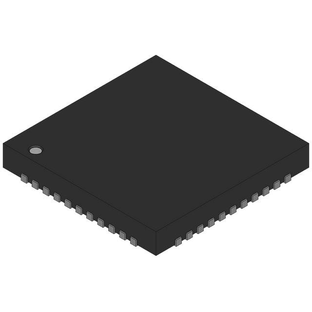
- Part No.:
- PEB2047NV2.1
- Manufacturer:
- Infineon Technologies
- Category:
- Specialized ICs
- Package:
- 44-LCC (J-Lead)
- Datasheet:
-
 PEB2047NV2.1.pdf
- Description:
- IC MEMORY 44PLCC
- Quantity:
- Payment:

- Shipping:

Inventory:106
Please send an inquiry. Send us your inquiry, and we will respond immediately.
Product details
Overview
PEB2047NV2.1 from Siemens AG is a non-blocking CMOS memory time switch large (MTSL) IC for PCM telecommunication systems, supporting 2048–16384 kbit/s data rates, 16 input/8 output PCM lines, and programmable per-slot channel delay with ±½-clock-step resolution. It operates on a single 5 V ±5 % supply and integrates µP interface (8-bit Motorola/Intel), built-in self-test, and tristate-capable output drivers for tandem expansion.
For engineers reviewing the PEB2047NV2.1 datasheet, PEB2047NV2.1 pinout, PEB2047NV2.1 application, or PEB2047NV2.1 equivalent, key selection criteria include frame-synchronized PCM switching capability, register-accessible delay calibration per input line, open-drain interrupt signaling, and LCC-44 surface-mount packaging compatible with legacy telecom timing architectures.
Technical Context
The PEB2047NV2.1 implements a time-space switch architecture optimized for constant-frame-delay operation in digital telephony infrastructure. It supports three device clock frequencies (4096/8192/16384 kHz), enables independent configuration of input and output modes, and provides individual line delay measurement for all eight PCM inputs via dedicated FSx pins.
Its µP interface operates in multiplexed (Intel/Motorola) or demultiplexed mode, with address/data bus sharing (AD0–AD7), chip-select (CS), read/write control (R/W or WR/RD), and address latch enable (ALE). The INT pin delivers active-low open-drain interrupt signals synchronized to frame boundaries.
Key Specifications
| Parameter | Value and Actual Design Meaning |
|---|---|
| Switch Capacity | Up to 1024 × 1024 PCM channels; enables full non-blocking time-slot interconnection in E1/T1 backbone nodes. |
| PCM Interface | 16 serial input lines (IN0–IN15), 8 tristatable output lines (OUT0–OUT7); supports FSx frame sync evaluation on IN8–IN15. |
| Device Clock | 4096 / 8192 / 16384 kHz; determines PCM bit rate and frame timing granularity for synchronous switching. |
| µP Interface | 8-bit multiplexed/demultiplexed bus; supports Intel (ALE-controlled) and Motorola (DS-controlled) protocols with CS, R/W, RD/WR. |
| Supply Voltage | 5 V ±5 %; single-rail operation eliminates need for dual supplies in telecom line cards. |
| Interrupt Output | Pin 6 (INT), active-low open-drain; allows wired-OR interrupt aggregation in multi-chip MTSL systems. |
| Package | P-LCC-44 (SMD); 44-pin plastic leaded chip carrier with gull-wing leads for reflow-compatible mounting. |
Pinout & Package
P-LCC-44 surface-mount package with 44 gull-wing leads; body size 16.6 mm × 16.6 mm, lead pitch 0.8 mm, JEDEC MS-026 compliant.
| Pin/Terminal | Circuit Role | Design Meaning |
|---|---|---|
| 1 | VSS | Ground reference for all internal logic and I/O circuits; must be low-impedance connection to system ground plane. |
| 3 | SP | Synchronization Pulse input; aligns internal frame counter to external PCM system timing reference. |
| 4–17, 19–20 | IN0–IN15 / FS0–FS7 | 16 bidirectional PCM input/frame sync terminals; IN0–IN7 are dedicated PCM data, IN8–IN15 serve dual role as PCM data or frame sync inputs. |
| 21–22 | A0, A1 | Register address bits for demultiplexed µP interface; select among 4 internal registers during CS-active cycles. |
| 22 | CS | Chip Select input; low level enables register access and disables output drivers during µP transactions. |
| 23 | VDD | Main power supply input; requires local 5 V ±5 % regulation and decoupling near pin. |
| 25 | R/W (Motorola) / WR (Intel) | Write control signal; defines direction of µP bus transfer during CS-active period. |
| 24 | DS (Motorola) / RD (Intel) | Data Strobe/Read signal; rising edge latches read data or validates write data timing. |
| 26–34 | AD0–AD7 | Multiplexed address/data bus; carries both register addresses and data in Intel/Motorola modes; shared with system bus in demultiplexed mode. |
| 35–38, 40–43 | OUT0–OUT7 | Tristatable PCM output drivers; support cascaded MTSL configurations and tandem switching without external buffers. |
| 39 | RES | Asynchronous reset input; high level forces internal state machines and registers into known initialization state. |
| 44 | CLK | Master device clock input; sets fundamental timing for PCM sampling, frame generation, and internal pipeline operation. |
| 2 | ALE | Address Latch Enable; controls external latch capture of AD0–AD7 address bits in Intel multiplexed mode. |
| 6 | INT (OD) | Open-drain interrupt output; sinks current when asserted; requires external pull-up for logic-level compatibility. |
Key Features
| Feature | Design Value |
|---|---|
| Per-time-slot delay programming | Enables constant frame delay across all switched channels by adjusting individual input line sampling phase in ½-clock-step increments. |
| Built-in self-test (BIST) | Verifies internal RAM integrity, register accessibility, and switching path functionality without external test equipment. |
| Tristate output capability | Allows direct wire-OR connection of multiple MTSL outputs for expanded channel count in tandem switching applications. |
| Frame-sync evaluation on input lines | Eight dedicated FSx inputs (IN8–IN15) permit real-time frame boundary detection and alignment without external logic. |
| Configurable µP interface | Supports both Intel (ALE + RD/WR) and Motorola (DS + R/W) bus protocols, enabling drop-in replacement in diverse legacy controller designs. |
Applications
| Digital Line Card Switching | E1/T1 Multiplexer Timing Control |
|---|---|
|
Use Scenario: Telecom line card handling 32-channel E1 streams with dynamic time-slot assignment between tributaries. IC Role / Device Role / Timing Role: Memory Time Switch Large (MTSL) performing non-blocking time-slot interchange with sub-microsecond latency. Use Value: Enables per-slot delay calibration to eliminate frame misalignment across distributed switching nodes in hierarchical networks. |
Use Scenario: Synchronizing multiple E1/T1 multiplexers to a common master clock while preserving payload integrity. IC Role / Device Role / Timing Role: Frame-aligned PCM switch providing deterministic channel-to-channel delay for jitter-sensitive transport layers. Use Value: Guarantees constant frame delay across all 1024 switched paths, preventing buffer overflow in downstream framer ICs. |
| Tandem Digital Cross-Connect System | Legacy PBX Time-Slot Reassignment |
|
Use Scenario: Interfacing two independent digital cross-connect systems requiring bidirectional PCM channel mapping. IC Role / Device Role / Timing Role: Tristate-enabled MTSL acting as transparent time-slot bridge between upstream/downstream switching fabrics. Use Value: Eliminates need for external bus transceivers by allowing direct parallel connection of multiple PEB2047 outputs to shared backplane. |
Use Scenario: Retrofitting analog PBX systems with digital trunk interfaces requiring flexible time-slot routing. IC Role / Device Role / Timing Role: Programmable time-switch IC interfacing with 80C31-based control processors via 8-bit parallel bus. Use Value: Supports in-operation bit-sampling adjustment without introducing bit errors-critical for maintaining voice quality during live reconfiguration. |
Equivalent & Alternatives
The following parts are listed as comparable options for similar memory time switch applications.
| Alternative Part | Technical Difference | Application Difference | Selection Advice |
|---|---|---|---|
| PEF2047-N-16 V2.1 | Same die, identical pinout and register map; differs only in ordering code and package marking (Q67100-H6301 vs Q67100-H6238). | Functionally identical; used interchangeably in production where Siemens part numbering conventions require suffix distinction. | Select PEF2047-N-16 only if procurement system mandates exact match to that ordering code; no electrical or functional trade-offs. |
| PEB2047-16 V2.1 | Same silicon, same LCC-44 package; differs solely in labeling-"PEB2047-16" denotes version with full 16384-kHz clock support enabled in firmware. | Required for systems operating at 16384-kHz device clock; PEB2047NV2.1 supports up to 8192 kHz unless explicitly marked "-16". | Choose PEB2047-16 only when 16384-kHz operation is mandatory; otherwise PEB2047NV2.1 meets all other specifications identically. |
Compared with PEF2047-N-16 and PEB2047-16, the PEB2047NV2.1 offers identical switching architecture and µP interface but excludes 16384-kHz clock mode activation-making it suitable for cost-optimized E1/T1 systems where maximum clock rate is not required.
Availability
PEB2047NV2.1 is available at Aetrix Electronics and suitable for digital line card switching, E1/T1 multiplexer timing control, tandem digital cross-connect systems, and legacy PBX time-slot reassignment requiring stable component supply and long-term obsolescence management.
Supply support for PEB2047NV2.1 includes scheduled delivery planning, volume procurement assistance, BOM continuity management, traceable sourcing, and lifecycle availability coordination for OEM customers, industrial embedded developers, connected-device designers, and electronics production programs.
Manufacturer
Siemens AG Semiconductor Group (now Infineon Technologies) was a leading European semiconductor manufacturer specializing in industrial, automotive, and telecommunications ICs before spinning off its chip business in 1999.
The PEB2047NV2.1 belongs to Siemens' MTSL (Memory Time Switch Large) product line, designed specifically for non-blocking PCM time-slot interchange in digital telephony infrastructure including central office switches and remote line concentrators.
FAQ
What µP bus protocols does the PEB2047NV2.1 support?
The PEB2047NV2.1 supports both Intel-type (with ALE, RD, WR) and Motorola-type (with DS, R/W) 8-bit parallel microprocessor interfaces. Configuration is determined by external wiring: ALE tied to VSS for Intel demultiplexed mode, or to VDD for Motorola demultiplexed mode. Multiplexed operation uses AD0–AD7 for both address and data.
Does the PEB2047NV2.1 support 16384-kHz operation?
No-the PEB2047NV2.1 supports device clock frequencies of 4096 kHz and 8192 kHz only. Full 16384-kHz capability is exclusive to the PEB2047-16 variant, as confirmed in the "Important Note" on page 6 of the 03.95 datasheet. Using PEB2047NV2.1 at 16384 kHz violates absolute maximum ratings and may cause functional failure.
How is frame synchronization implemented on the PEB2047NV2.1?
Frame synchronization is achieved via the SP (Synchronization Pulse) input (Pin 3) and eight configurable FSx inputs mapped to IN8–IN15. These allow real-time frame boundary detection on selected PCM inputs. The STAR register (Status Register) provides flags indicating frame alignment status and error conditions for each monitored line.
What is the function of the INT pin, and how should it be interfaced?
Pin 6 (INT) is an active-low open-drain interrupt output. It asserts when internal events occur-such as completion of indirect register access or frame boundary detection-and requires an external pull-up resistor (typically 4.7 kΩ to VDD) to generate a valid logic-high level. Multiple PEB2047 devices can share a single interrupt line via wired-OR connection.
PEB2047NV2.1 Specifications
- Product attributes
- Attribute value
- Manufacturer:
- Infineon Technologies
- Series:
- -
- Package/Case:
- 44-LCC (J-Lead)
- Packaging:
- Bulk
- Product Status:
- Active
- Programmable:
- Not Verified
- Type:
- Memory
- Applications:
- -
- Mounting Type:
- Surface Mount
- Supplier Device Package:
- 44-PLCC (16.6x16.6)
- Grade:
- -
- Qualification:
- -
PEB2047NV2.1 FAQ
1.How can I place an order for PEB2047NV2.1 through Aetrix?
Please submit a Request for Quotation (RFQ) for PEB2047NV2.1 on Aetrix. Our sales agent will provide a competitive quotation and guide you through the order confirmation once you accept the terms.
2.Are the price and stock information for PEB2047NV2.1 reliable?
The price and inventory of PEB2047NV2.1 are updated periodically and may fluctuate due to market conditions. Stock and pricing data are typically refreshed every 24 hours. Quotation validity for PEB2047NV2.1 is usually 5 days.
3.What payment methods are accepted for PEB2047NV2.1?
We accept Wire Transfer, PayPal, Credit Card, Western Union, MoneyGram, and Escrow for PEB2047NV2.1 transactions.
Note: Certain payment methods may incur a processing fee.
4.How is shipping managed for PEB2047NV2.1?
PEB2047NV2.1 orders can be shipped via leading logistics carriers, including DHL, UPS, FedEx, TNT, or Registered Mail.
Once your PEB2047NV2.1 order is processed, you will receive an email with the shipment details and tracking number.
Note: Tracking information may take up to 24 hours to appear. Express delivery typically takes 3–5 business days.
5.How can I obtain technical support or documentation for PEB2047NV2.1?
For technical support, including PEB2047NV2.1 datasheets, pinout diagrams, or application guidance, please contact our engineering support team. They can provide detailed documentation and assistance for your PEB2047NV2.1 requirements.
6.How does Aetrix verify that PEB2047NV2.1 is sourced from the original manufacturer or authorized distributors?
All PEB2047NV2.1 products on Aetrix are procured from qualified distributors and authorized channels. Our dedicated quality assurance team conducts strict verification, including traceability checks and, if necessary, third-party testing. This ensures that PEB2047NV2.1 meets industry standards.
7.What is the process for return or replacement of PEB2047NV2.1?
All PEB2047NV2.1 units undergo pre-shipment inspection (PSI). If there is an issue with PEB2047NV2.1, returns or replacements are accepted under the following conditions:
1.Quantity discrepancies, incorrect items, or visible external defects (such as breakage or corrosion), acknowledged by Aetrix.
2.The issue is reported within 90 days of delivery.
3.The PEB2047NV2.1 part is unused and in its original packaging.
Return procedure for PEB2047NV2.1:
1.Submit a request within 90 days.
2.Obtain a Return Material Authorization (RMA) from Aetrix.
PEB2047NV2.1 Tags

-
CAP200DG-TL
Power Integrations
-
ATSHA204A-MAHDA-T
Microchip Technology

-
ATSHA204A-SSHDA-T
Microchip Technology

-
ATSHA204A-STUCZ-T
Microchip Technology
-
ATECC608B-MAHDA-T
Microchip Technology
-
ATECC608B-MAHCZ-S
Microchip Technology

-
ATECC608B-SSHDA-T
Microchip Technology
-
ATECC608B-MAHDA-S
Microchip Technology
-
ATECC608A-MAHDA-S
Microchip Technology
-
ATECC608B-MAVDA-T
Microchip Technology

-
ATECC608A-SSHDA-T
Microchip Technology
-
ATECC508A-MAHDA-T
Microchip Technology
Tech Hub

Operational amplifier guide covering op amp basics, feedback, ideal vs real op amps, common configurations, buffer circuits, offset, bias current, gain-bandwidth, slew rate, rail-to-rail limits and sel…

Jumper cables guide covering safe connection order, red and black clamp placement, final ground connection, cable gauge, length, clamp quality, copper vs CCA cables, jump starter comparison and battery…

LDO regulator guide covering low dropout voltage, power dissipation, thermal design, PSRR, output noise, capacitor stability, adjustable LDO circuits, LDO vs buck converter and datasheet selection chec…

Conditional Access Module guide covering CAM meaning, CI/CI+ interface, smart card authorization, DVB security workflow, TV and set-top box compatibility, internal electronics, ESD protection, connecto…

Guide to electronic component obsolescence covering EOL risk, PCN/PDN notices, last-time buy planning, replacement options, form-fit-function validation, counterfeit risk and BOM lifecycle management.

18650 battery guide covering lithium-ion cell basics, 3.6V/3.7V voltage, 4.2V charging, mAh and Wh capacity, protected cells, chargers, BMS, series-parallel packs, holders, welding and sourcing checks.…

Hall effect sensor guide covering working principle, linear and digital sensors, Arduino circuits, current sensing, speed detection, automotive applications, A3144 examples, signal filtering and datash…

Product Change Notification guide for electronic components, covering PCN meaning, PCN vs PDN/EOL, common change types, risk levels, form-fit-function review, engineering validation, BOM control, LTB/L…

A practical guide to blend door actuators, covering HVAC function, symptoms, location, AC and heater issues, reset and calibration, replacement cost, electrical diagnosis, compatibility checks, and rep…

Engineering guide to Raspberry Pi alternatives, covering chip-level differences, Orange Pi, ROCK, Jetson, Banana Pi, NanoPi, Compute Module, Pico, GPIO, camera, HAT compatibility, and replacement risks…


