
 My Inquiry
 My Account


Infineon Technologies PEB2447H-V12
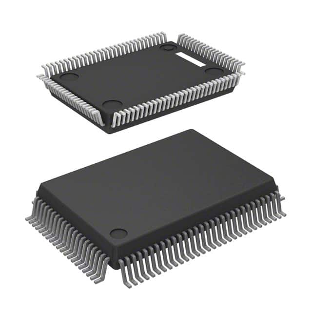
- Part No.:
- PEB2447H-V12
- Manufacturer:
- Infineon Technologies
- Category:
- Specialized
- Package:
- 100-BQFP
- Datasheet:
-
 PEB2447H-V12.pdf
- Description:
- IC INTERFACE SPECIALIZED 100MQFP
- Quantity:
- Payment:

- Shipping:

Inventory:2,800
Please send an inquiry. Send us your inquiry, and we will respond immediately.
Product details
Overview
PEB2447H-V12 from Siemens AG is a monolithic CMOS Memory Time Switch Extended Large (MTSXL) device for PCM telecommunication systems, functioning as a non-blocking 2048×2048 time/space switch with 32 input and 32 output PCM lines, 16.384 MHz device clock, TTL-compatible I/O, and IEEE 1149.1 boundary scan support - deployed in digital switching infrastructure for frame-aligned channel routing.
For engineers reviewing the PEB2447H-V12 datasheet, PEB2447H-V12 pinout, PEB2447H-V12 application, or PEB2447H-V12 equivalent, key selection criteria include PCM frame delay compensation capability, real-time input offset reprogramming without bit errors, tristate expansion support, built-in selftest via boundary scan, and Intel-type 8-bit demultiplexed µP interface compatibility.
Technical Context
The PEB2447H-V12 implements a fully non-blocking time-slot interconnection architecture for 4.096/8.192 Mbit/s PCM systems, using on-chip connection and data memory accessed via an 8-bit Intel-demultiplexed microprocessor interface. It supports dynamic frame alignment through programmable input offsets for 16 PCM inputs and individual line delay measurement on six dedicated FS inputs.
Its boundary-scan TAP controller complies fully with IEEE 1149.1, enabling test access to internal registers and built-in selftest (BIST) execution. The device guarantees glitch-free reconfiguration of input sampling points during operation - critical for maintaining bit integrity in live PCM traffic paths.
Key Specifications
| Parameter | Value and Actual Design Meaning |
|---|---|
| Switch Capacity | 2048 × 2048 non-blocking PCM time slots - enables full-mesh channel routing in large-scale digital exchanges. |
| PCM Interface | 32 input + 32 output TTL-compatible serial PCM lines - directly interfaces standard E1/T1 framing hardware. |
| Device Clock | 16.384 MHz - precisely matches 2× E1 frame rate (2.048 MHz × 8), ensuring synchronous time-slot alignment. |
| Input Offset Control | Programmable per-channel offset for 16 inputs - compensates variable line propagation delays without service interruption. |
| Frame Measurement Inputs | 6 dedicated FS0–FS5 pins - measure frame wander across multiple PCM links for adaptive synchronization. |
| µP Interface | 8-bit Intel-demultiplexed bus (A0–A4, RD, WR, CS, D0–D7) - integrates with legacy 80Cxx/8051-based control planes. |
| Built-in Selftest | Fully accessible via boundary scan or µP command - validates internal memory, register access, and clock path integrity. |
Pinout & Package
PEB2447H-V12 is housed in a P-MQFP-100-2 (Plastic Metric Quad Flat Package, 100-pin, 0.5 mm pitch) with exposed thermal pad. Pin 1 marked by index notch; leads are lead-free and RoHS-compliant per Siemens 1997 manufacturing standards.
| Pin/Terminal | Circuit Role | Design Meaning |
|---|---|---|
| IN0–IN31 | PCM Serial Input | 32 TTL-level serial data inputs accepting 2.048 MHz or 4.096 MHz PCM streams - mapped to time-slot matrix rows. |
| OUT0–OUT31 | PCM Serial Output | 32 TTL-level serial outputs delivering switched time-slot data - driven with controlled slew rate for EMI reduction. |
| FS0–FS5 | Frame Sync Measurement | 6 dedicated frame-synchronization inputs used for real-time delay measurement and wander compensation. |
| CLK | Master Device Clock | 16.384 MHz input driving all internal timing - must be low-jitter to prevent bit misalignment in high-density switching. |
| SP | Synchronization Pulse | External system sync pulse aligning internal frame boundaries - enables multi-device phase coherence in tandem configurations. |
| A0–A4, CS, RD, WR, D0–D7 | µP Interface Bus | Intel-demultiplexed 8-bit address/data/control interface - allows direct register read/write without external glue logic. |
| TCK, TMS, TDI, TDO | JTAG Boundary Scan | IEEE 1149.1-compliant test access port - enables production testing, in-system diagnostics, and BIST activation. |
| VDD / VSS | Power Supply | Single 5 V ±5% supply with distributed decoupling pads - requires local 100 nF ceramic + 10 µF tantalum per power pair. |
Key Features
| Feature | Design Value |
|---|---|
| In-operation input offset reprogramming | Adjusts PCM frame sampling point dynamically without introducing bit errors - essential for maintaining BER <10⁻¹² in live networks. |
| Tristate output enable | Allows cascading multiple PEB2447H-V12 devices on shared PCM buses - supports tandem switching and capacity scaling. |
| Half-clock-step programmable clock shift | Enables fine-grained skew adjustment (±0.5 × 61.035 ns) on input/output clocks - corrects sub-bit-period timing mismatches. |
| 6-channel frame evaluation | Dedicated FS0–FS5 inputs measure frame arrival variance across diverse physical links - feeds adaptive delay compensation algorithm. |
| Direct register addressing | All 17 internal registers (MODR, CMDR, STAR, etc.) accessible via A0–A4 and CS/RD/WR - eliminates indirect addressing overhead. |
Applications
| PCM Digital Exchange Core | Multi-Node Tandem Switching |
|---|---|
|
Use Scenario: Central switching fabric in Class-5 digital telephone exchanges handling 2048 concurrent E1 channels. IC Role / Device Role / Timing Role: Non-blocking time-slot interchanger synchronizing incoming/outgoing PCM frames with sub-bit precision. Use Value: Enables carrier-grade call setup latency <10 ms and zero-frame-loss handover between trunk groups. |
Use Scenario: Cascaded switching nodes in regional telecom backbone connecting geographically dispersed central offices. IC Role / Device Role / Timing Role: Frame-aligned tandem switch supporting synchronized delay compensation across multi-hop PCM paths. Use Value: Maintains end-to-end jitter <1.5 UI and eliminates cumulative frame slip in >3-node chains. |
| SONET/SDH Add-Drop Multiplexer | Legacy PBX Expansion Module |
|
Use Scenario: DS1/E1 tributary grooming stage in SONET OC-3/OC-12 ADMs interfacing legacy circuit-switched networks. IC Role / Device Role / Timing Role: Time-slot mapper converting asynchronous DS1 feeds into synchronous STS-1 payloads with deterministic latency. Use Value: Achieves <±25 ppm frequency tolerance tracking and seamless hitless protection switching. |
Use Scenario: Modular time-slot expansion card for enterprise PBX systems upgrading analog-to-digital trunk capacity. IC Role / Device Role / Timing Role: Plug-in PCM switch providing hot-swappable 32×32 channel routing under µP supervision. Use Value: Delivers field-upgradable port density without firmware rewrite or backplane redesign. |
Equivalent & Alternatives
The following parts are listed as comparable options for similar time-slot switching applications.
| Alternative Part | Technical Difference | Application Difference | Selection Advice |
|---|---|---|---|
| PEB2047H | Smaller 1024×1024 capacity; no FS0–FS5 frame measurement inputs; identical µP interface and clock architecture. | Limited to medium-scale exchanges or single-node PBX; lacks multi-link wander compensation. | Select when system scale ≤1024 channels and frame delay variation is negligible across links. |
| MT8985D1 | 2048×2048 switch but uses serial SPI µP interface; no built-in BIST; requires external frame sync logic. | Higher µP overhead for register access; unsuitable for safety-critical diagnostics without added test firmware. | Prefer only if board space constraints prohibit 100-pin MQFP and SPI integration is already standardized. |
Compared with PEB2447H-V12, PEB2047H reduces cost and power at the expense of scalability and adaptive synchronization, while MT8985D1 trades diagnostic robustness and parallel interface simplicity for package compactness - making PEB2447H-V12 optimal for carrier-class reliability and real-time frame integrity.
Availability
PEB2447H-V12 is available at Aetrix Electronics and suitable for PCM digital exchange cores, multi-node tandem switching, SONET/SDH add-drop multiplexers, and legacy PBX expansion modules requiring stable component supply and long-term lifecycle support.
Supply support for PEB2447H-V12 includes scheduled delivery planning, volume procurement assistance, BOM continuity management, traceable sourcing, and lifecycle availability coordination for OEM customers, industrial embedded developers, connected-device designers, and electronics production programs.
Manufacturer
Siemens AG Semiconductor Group (now Infineon Technologies) was a leading European semiconductor manufacturer specializing in industrial, telecom, and automotive ICs before its semiconductor division spun off in 1999.
The MTSXL product line - including PEB2447H-V12 - was engineered specifically for carrier-grade digital telephony infrastructure, emphasizing deterministic timing, fault-tolerant configuration, and seamless integration into legacy µP-controlled switching systems.
FAQ
What is the maximum supported PCM data rate per input/output line?
The PEB2447H-V12 supports two standard rates: 2.048 Mbit/s (E1) and 4.096 Mbit/s (double-E1). Each INx/OUTx line operates at one of these fixed rates - selected via external configuration and verified by the 16.384 MHz master clock (exactly 8× 2.048 MHz). No oversampling or rate adaptation is performed internally.
Does PEB2447H-V12 support hot insertion or live reconfiguration?
Yes - input offset registers can be rewritten during active PCM traffic without causing bit errors or frame loss. This is guaranteed by internal handshake logic that stalls switching matrix updates until frame boundaries, preserving bit integrity. Full device reset (via RES pin) still requires service interruption.
How is frame synchronization maintained across multiple PEB2447H-V12 devices?
Multiple units synchronize via the SP (Synchronization Pulse) input and shared CLK signal. When cascaded, one device acts as master SP source while others use SP as input; FS0–FS5 measurements feed a centralized delay compensation algorithm running on the host µP - not on-chip.
Is the PEB2447H-V12 compliant with modern RoHS or REACH requirements?
Originally manufactured in 1997 under Siemens' pre-RoHS process, the PEB2447H-V12 contains leaded solder in its P-MQFP-100-2 package. Aetrix Electronics supplies only tested, traceable legacy stock meeting original Siemens specifications - not RoHS-compliant re-manufactured versions.
PEB2447H-V12 Specifications
- Product attributes
- Attribute value
- Manufacturer:
- Infineon Technologies
- Series:
- -
- Package/Case:
- 100-BQFP
- Packaging:
- Tray
- Product Status:
- Obsolete
- Applications:
- Memory Time Switch
- Interface:
- -
- Voltage - Supply:
- -
- Supplier Device Package:
- PG-MQFP-100-2
- Grade:
- -
- Qualification:
- -
- Mounting Type:
- Surface Mount
PEB2447H-V12 FAQ
1.How can I place an order for PEB2447H-V12 through Aetrix?
Please submit a Request for Quotation (RFQ) for PEB2447H-V12 on Aetrix. Our sales agent will provide a competitive quotation and guide you through the order confirmation once you accept the terms.
2.Are the price and stock information for PEB2447H-V12 reliable?
The price and inventory of PEB2447H-V12 are updated periodically and may fluctuate due to market conditions. Stock and pricing data are typically refreshed every 24 hours. Quotation validity for PEB2447H-V12 is usually 5 days.
3.What payment methods are accepted for PEB2447H-V12?
We accept Wire Transfer, PayPal, Credit Card, Western Union, MoneyGram, and Escrow for PEB2447H-V12 transactions.
Note: Certain payment methods may incur a processing fee.
4.How is shipping managed for PEB2447H-V12?
PEB2447H-V12 orders can be shipped via leading logistics carriers, including DHL, UPS, FedEx, TNT, or Registered Mail.
Once your PEB2447H-V12 order is processed, you will receive an email with the shipment details and tracking number.
Note: Tracking information may take up to 24 hours to appear. Express delivery typically takes 3–5 business days.
5.How can I obtain technical support or documentation for PEB2447H-V12?
For technical support, including PEB2447H-V12 datasheets, pinout diagrams, or application guidance, please contact our engineering support team. They can provide detailed documentation and assistance for your PEB2447H-V12 requirements.
6.How does Aetrix verify that PEB2447H-V12 is sourced from the original manufacturer or authorized distributors?
All PEB2447H-V12 products on Aetrix are procured from qualified distributors and authorized channels. Our dedicated quality assurance team conducts strict verification, including traceability checks and, if necessary, third-party testing. This ensures that PEB2447H-V12 meets industry standards.
7.What is the process for return or replacement of PEB2447H-V12?
All PEB2447H-V12 units undergo pre-shipment inspection (PSI). If there is an issue with PEB2447H-V12, returns or replacements are accepted under the following conditions:
1.Quantity discrepancies, incorrect items, or visible external defects (such as breakage or corrosion), acknowledged by Aetrix.
2.The issue is reported within 90 days of delivery.
3.The PEB2447H-V12 part is unused and in its original packaging.
Return procedure for PEB2447H-V12:
1.Submit a request within 90 days.
2.Obtain a Return Material Authorization (RMA) from Aetrix.
PEB2447H-V12 Tags

-
NVT4857UKAZ
NXP USA Inc.

-
TCA8418RTWR
Texas Instruments

-
PCA9546APWR
Texas Instruments

-
MD0100N8-G
Microchip Technology

-
PCA9548APW,118
NXP USA Inc.

-
PCA9540BDP,118
NXP USA Inc.

-
PCA9548APWR
Texas Instruments

-
PCA9546APW,118
NXP USA Inc.

-
PTN3360DBS,518
NXP USA Inc.

-
PCA9546ABS,118
NXP USA Inc.

-
PCA9518PWR
Texas Instruments

-
PCA9545APW,118
NXP USA Inc.
Tech Hub

An engineering guide to LED driver operation, constant-current and constant-voltage outputs, linear and switching topologies, dimming, IC selection, calculations, replacement compatibility, and fault c…

Operational amplifier guide covering op amp basics, feedback, ideal vs real op amps, common configurations, buffer circuits, offset, bias current, gain-bandwidth, slew rate, rail-to-rail limits and sel…

Jumper cables guide covering safe connection order, red and black clamp placement, final ground connection, cable gauge, length, clamp quality, copper vs CCA cables, jump starter comparison and battery…

LDO regulator guide covering low dropout voltage, power dissipation, thermal design, PSRR, output noise, capacitor stability, adjustable LDO circuits, LDO vs buck converter and datasheet selection chec…

Conditional Access Module guide covering CAM meaning, CI/CI+ interface, smart card authorization, DVB security workflow, TV and set-top box compatibility, internal electronics, ESD protection, connecto…

Guide to electronic component obsolescence covering EOL risk, PCN/PDN notices, last-time buy planning, replacement options, form-fit-function validation, counterfeit risk and BOM lifecycle management.

18650 battery guide covering lithium-ion cell basics, 3.6V/3.7V voltage, 4.2V charging, mAh and Wh capacity, protected cells, chargers, BMS, series-parallel packs, holders, welding and sourcing checks.…

Hall effect sensor guide covering working principle, linear and digital sensors, Arduino circuits, current sensing, speed detection, automotive applications, A3144 examples, signal filtering and datash…

Product Change Notification guide for electronic components, covering PCN meaning, PCN vs PDN/EOL, common change types, risk levels, form-fit-function review, engineering validation, BOM control, LTB/L…

A practical guide to blend door actuators, covering HVAC function, symptoms, location, AC and heater issues, reset and calibration, replacement cost, electrical diagnosis, compatibility checks, and rep…


