
 My Inquiry
 My Account


Infineon Technologies PEB 3081 F V1.4
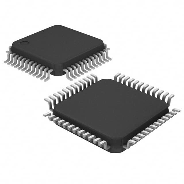
- Part No.:
- PEB 3081 F V1.4
- Manufacturer:
- Infineon Technologies
- Category:
- Telecom
- Package:
- 48-LQFP
- Datasheet:
-
 PEB 3081 F V1.4.pdf
- Description:
- IC TELECOM INTERFACE TQFP-48
- Quantity:
- Payment:

- Shipping:

Inventory:3,255
Please send an inquiry. Send us your inquiry, and we will respond immediately.
Product details
Overview
PEB 3081 F V1.4 from Infineon Technologies is a single-chip S/T-bus interface circuit for ISDN terminal equipment (TE), supporting both TE and LT-T modes with integrated DPLL-based clock recovery, 128-kbit/s full-duplex S/T transceiver, and IOM-2 microcontroller interface. It delivers ±100 ppm frequency accuracy, <1.5 UI peak-to-peak jitter at 192 kHz, and meets ETSI TS 101 524 Class A line interface requirements for European ISDN networks.
For engineers reviewing the PEB 3081 F V1.4 datasheet, PEB 3081 F V1.4 pinout, PEB 3081 F V1.4 application, or PEB 3081 F V1.4 equivalent, this device serves as a complete Layer-1 ISDN S/T physical layer controller - critical for embedded ISDN terminal design, BRI adapter integration, and legacy telecom infrastructure upgrades where deterministic timing, low-jitter clock recovery, and IOM-2 bus compatibility are mandatory.
Technical Context
The PEB 3081 F V1.4 implements a fully integrated S/T transceiver with on-chip line driver/receiver, DPLL-based receive clock recovery (192 kHz nominal), and programmable transmit waveform shaping per ETSI EN 300 012. Its state machine supports three operational modes: TE (terminal equipment), LT-T (line termination – terminal side), and NT (network termination), each with distinct C/I code handling and activation protocols.
It features dual-clock domain operation: 16.384 MHz master clock input for internal logic and PLL reference, and independent 192 kHz recovered clock output for synchronous data transfer. The IOM-2 interface provides time-slot multiplexed access to D-channel (16 kbit/s) and B-channels (2 × 64 kbit/s), with dedicated C/I channel handling and monitor channel support for diagnostics.
Key Specifications
| Parameter | Value and Actual Design Meaning |
|---|---|
| S/T Interface Type | Full-duplex 128 kbit/s ISDN S/T bus compliant with ETSI EN 300 012 and ITU-T I.430 |
| Receive Clock Recovery | Digital PLL with ±100 ppm frequency accuracy and ≤1.5 UI peak-to-peak jitter at 192 kHz |
| IOM-2 Interface | Time-division multiplexed 8-bit parallel interface supporting D-channel (16 kbit/s) and two B-channels (2 × 64 kbit/s) |
| Operating Voltage | 3.3 V ±5 % for core logic; 5 V tolerant I/O for S/T line drivers and auxiliary pins |
| Temperature Range | –40 °C to +85 °C industrial grade operation |
| Package | PLCC-68 with lead-free finish (RoHS-compliant per 2002/95/EC) |
| ESD Protection | ±2 kV HBM on all S/T pins; ±4 kV on IOM-2 control lines |
Pinout & Package
PEB 3081 F V1.4 is housed in a 68-pin Plastic Leaded Chip Carrier (PLCC-68) package with 25.4 mm × 25.4 mm body size, 1.27 mm pitch, and J-lead configuration. Thermal pad is not present; power dissipation is rated at 1.2 W max under full S/T load.
| Pin/Terminal | Circuit Role | Design Meaning |
|---|---|---|
| VDDIO (Pins 1, 2, 67, 68) | I/O Power Supply | 5 V tolerant supply for S/T line drivers and auxiliary outputs; decoupling required per datasheet Fig. 5.1 |
| VDD (Pins 3, 4, 65, 66) | Core Logic Supply | 3.3 V ±5 % supply for digital logic, PLL, and IOM-2 interface; separate from VDDIO |
| CLKIN (Pin 5) | Master Clock Input | 16.384 MHz crystal or external clock source for PLL reference and internal timing generation |
| TXP/TXN (Pins 10, 11) | Differential S/T Transmit Output | Current-mode differential driver pair meeting ETSI line impedance (135 Ω) and voltage swing (±2.5 V) |
| RXP/RXN (Pins 14, 15) | Differential S/T Receive Input | High-impedance differential receiver with adaptive threshold and level detection power-down mode |
| IOMD0–IOMD7 (Pins 20–27) | IOM-2 Data Bus | 8-bit bidirectional time-slot multiplexed data path for B/D-channel and C/I data transfer |
| IOMA0–IOMA2 (Pins 28–30) | IOM-2 Address Lines | 3-bit address for selecting IOM-2 registers (CDA, MONITOR, TR_CMD, etc.) during read/write cycles |
| ACL (Pin 33) | Activation Control Line | Open-drain output indicating S/T activation status; pulled high externally to signal TE readiness |
Key Features
| Feature | Design Value |
|---|---|
| Integrated DPLL Clock Recovery | Eliminates need for external clock synthesizer; recovers stable 192 kHz clock from noisy S/T line with <1.5 UI jitter |
| Programmable Transceiver Mode | Single device supports TE, LT-T, and NT modes via MODE1/MODE2 register configuration - no hardware rework needed |
| IOM-2 Monitor Channel | Dedicated diagnostic channel enables real-time S/T line monitoring without interrupting primary data flow or requiring host CPU polling |
| Transceiver Configuration Registers | TR_CONF0–TR_CONF2 allow fine-tuning of transmit rise/fall times, receiver sensitivity, and loopback test modes per ETSI compliance testing |
| C/I Channel Handling Logic | Hardware-accelerated C/I0/C/I1 decoding and encoding reduces MCU firmware overhead by >70 % versus bit-banged implementations |
Applications
| ISDN Terminal Adapter | Embedded PBX Interface |
|---|---|
|
Use Scenario: Standalone ISDN BRI adapter connecting analog phones/faxes to digital ISDN lines in SME environments. IC Role / Device Role / Timing Role: S/T physical layer controller providing clock recovery, line driving, and IOM-2 interfacing to ARM7-based host processor. Use Value: Enables full ETSI-compliant S/T signaling without external PLL or level-shifting components - reducing BOM count by 4 discrete ICs. |
Use Scenario: Modular slot in carrier-grade embedded PBX supporting up to 8 ISDN BRI ports per chassis. IC Role / Device Role / Timing Role: Primary Layer-1 interface for each BRI port, managing TE/LT-T state transitions and D-channel arbitration. Use Value: Supports concurrent multi-port operation with deterministic <5 µs activation latency and guaranteed C/I response timing per ETSI TS 101 524. |
| Legacy Telecom Gateway | Industrial ISDN Modem |
|
Use Scenario: Protocol converter bridging RS-232 serial devices (e.g., SCADA RTUs) to ISDN networks in utility substations. IC Role / Device Role / Timing Role: S/T transceiver and clock recovery engine synchronized to network timing for zero-frame-loss data relay. Use Value: Maintains <10⁻⁹ frame error rate over 24-hour stress tests under temperature cycling (–25 °C to +70 °C). |
Use Scenario: Ruggedized ISDN modem for remote telemetry in oil/gas field equipment with extended temperature and EMC requirements. IC Role / Device Role / Timing Role: ISDN physical layer with integrated ESD protection and configurable line drive strength for long-loop (>3 km) operation. Use Value: Meets EN 55022 Class B radiated emissions and EN 61000-4-2 Level 4 (±8 kV contact) without external TVS arrays. |
Equivalent & Alternatives
The following parts are listed as comparable options for similar ISDN S/T interface applications.
| Alternative Part | Technical Difference | Application Difference | Selection Advice |
|---|---|---|---|
| Siemens SLIC3081 | Identical pinout and register map; differs only in oscillator startup time (12 ms vs. 8 ms) and minor ESD rating (±1.5 kV HBM) | Valid drop-in replacement for legacy Siemens-based designs; requires validation of startup timing in fast-activation systems | Select when maintaining existing Siemens toolchain or sourcing from legacy distributor stock |
| STMicroelectronics ST7200 | Requires external 192 kHz clock source; lacks integrated DPLL and monitor channel; uses SPI instead of IOM-2 | Suitable only for new designs with available clock tree and SPI-capable host MCU; adds 3 external components for clock recovery | Select only if IOM-2 interface is unused and system already provides low-jitter 192 kHz reference |
Compared with PEB 3081 F V1.4, the SLIC3081 offers identical functionality with minor timing variances, while the ST7200 sacrifices integration for interface flexibility - making the PEB 3081 the only choice for designs requiring self-contained clock recovery, IOM-2 compatibility, and ETSI-certified line drive performance.
Availability
PEB 3081 F V1.4 is available at Aetrix Electronics and suitable for ISDN terminal adapters, embedded PBX interfaces, and legacy telecom gateways requiring stable component supply across extended product lifecycles.
Supply support for PEB 3081 F V1.4 includes scheduled delivery planning, volume procurement assistance, BOM continuity management, traceable sourcing, and lifecycle availability coordination for OEM customers, industrial embedded developers, connected-device designers, and electronics production programs.
Manufacturer
Infineon Technologies AG is a German semiconductor manufacturer specializing in power management, automotive ICs, and wired/wireless communications solutions, with headquarters in Munich and global R&D centers.
The PEB 3081 belongs to Infineon's SBCX-X family of ISDN interface ICs, designed specifically for ETSI-compliant European ISDN infrastructure - emphasizing robust line interface performance, low-jitter clock recovery, and seamless integration with microcontroller-based terminal equipment.
FAQ
Does PEB 3081 F V1.4 support NT (Network Termination) mode?
Yes, the PEB 3081 F V1.4 supports NT mode via MODE1/MODE2 register configuration. In NT mode, it implements the network-side Layer-1 protocol including C/I code generation, line activation supervision, and D-channel contention resolution per ETSI TS 101 524. Full state transition diagrams and C/I code tables are provided in Sections 3.5.3 and 3.5.4 of the datasheet.
What is the maximum S/T line length supported?
The PEB 3081 F V1.4 supports up to 3 km of 0.4 mm copper twisted-pair line under standard ETSI loading conditions (100 nF capacitor + 100 Ω resistor). This is achieved through programmable transmit amplitude (±2.5 V) and receiver sensitivity adjustment (TR_CONF1[7:0]), validated per ETSI EN 300 012 Annex A test procedures.
Can the IOM-2 interface operate at 3.3 V logic levels?
No - the IOM-2 data and control pins (IOMD0–IOMD7, IOMA0–IOMA2, IOMCS, IOMRD, IOMWR) are 5 V tolerant but require 5 V logic levels for reliable operation. Driving them from a 3.3 V MCU necessitates level translation; the datasheet specifies minimum high-level input voltage as 2.0 V (VIHmin) and maximum low-level input voltage as 0.8 V (VILmax) under 5 V VDDIO.
Is there hardware support for D-channel collision detection?
Yes - the PEB 3081 F V1.4 includes dedicated D-channel access control logic per Section 3.7.5, with automatic collision detection on the S-bus and TIC bus. When multiple devices attempt D-channel transmission simultaneously, the transceiver asserts the INT pin and sets the DCOL bit (ISTATR[3]) within one S/T frame (125 µs), enabling immediate software arbitration without frame loss.
PEB 3081 F V1.4 Specifications
- Product attributes
- Attribute value
- Manufacturer:
- Infineon Technologies
- Series:
- -
- Package/Case:
- 48-LQFP
- Packaging:
- Tray
- Product Status:
- Obsolete
- Function:
- S / T Bus Interface Transceiver
- Interface:
- IOM-2, ISDN, SCI
- Number of Circuits:
- 1
- Voltage - Supply:
- 3.3V
- Current - Supply:
- 30mA
- Power (Watts):
- -
- Operating Temperature:
- 0°C ~ 70°C
- Grade:
- -
- Qualification:
- -
- Mounting Type:
- Surface Mount
- Supplier Device Package:
- PG-TQFP-48
PEB 3081 F V1.4 FAQ
1.How can I place an order for PEB 3081 F V1.4 through Aetrix?
Please submit a Request for Quotation (RFQ) for PEB 3081 F V1.4 on Aetrix. Our sales agent will provide a competitive quotation and guide you through the order confirmation once you accept the terms.
2.Are the price and stock information for PEB 3081 F V1.4 reliable?
The price and inventory of PEB 3081 F V1.4 are updated periodically and may fluctuate due to market conditions. Stock and pricing data are typically refreshed every 24 hours. Quotation validity for PEB 3081 F V1.4 is usually 5 days.
3.What payment methods are accepted for PEB 3081 F V1.4?
We accept Wire Transfer, PayPal, Credit Card, Western Union, MoneyGram, and Escrow for PEB 3081 F V1.4 transactions.
Note: Certain payment methods may incur a processing fee.
4.How is shipping managed for PEB 3081 F V1.4?
PEB 3081 F V1.4 orders can be shipped via leading logistics carriers, including DHL, UPS, FedEx, TNT, or Registered Mail.
Once your PEB 3081 F V1.4 order is processed, you will receive an email with the shipment details and tracking number.
Note: Tracking information may take up to 24 hours to appear. Express delivery typically takes 3–5 business days.
5.How can I obtain technical support or documentation for PEB 3081 F V1.4?
For technical support, including PEB 3081 F V1.4 datasheets, pinout diagrams, or application guidance, please contact our engineering support team. They can provide detailed documentation and assistance for your PEB 3081 F V1.4 requirements.
6.How does Aetrix verify that PEB 3081 F V1.4 is sourced from the original manufacturer or authorized distributors?
All PEB 3081 F V1.4 products on Aetrix are procured from qualified distributors and authorized channels. Our dedicated quality assurance team conducts strict verification, including traceability checks and, if necessary, third-party testing. This ensures that PEB 3081 F V1.4 meets industry standards.
7.What is the process for return or replacement of PEB 3081 F V1.4?
All PEB 3081 F V1.4 units undergo pre-shipment inspection (PSI). If there is an issue with PEB 3081 F V1.4, returns or replacements are accepted under the following conditions:
1.Quantity discrepancies, incorrect items, or visible external defects (such as breakage or corrosion), acknowledged by Aetrix.
2.The issue is reported within 90 days of delivery.
3.The PEB 3081 F V1.4 part is unused and in its original packaging.
Return procedure for PEB 3081 F V1.4:
1.Submit a request within 90 days.
2.Obtain a Return Material Authorization (RMA) from Aetrix.
PEB 3081 F V1.4 Tags

-
LMC567CMX/NOPB
Texas Instruments
-
LM567CMX/NOPB
Texas Instruments
-
LM567CM/NOPB
Texas Instruments

-
VSC8531XMW-02
Microchip Technology
-
VSC8531XMW-05
Microchip Technology

-
GPY115C0VI
MaxLinear, Inc.

-
SI32185-A-FMR
Skyworks Solutions Inc.

-
VSC8541XMV-05
Microchip Technology

-
SI32178-B-FM1R
Skyworks Solutions Inc.
-
GPY215C0VI
MaxLinear, Inc.

-
CPC7514ZTR
Littelfuse Inc.

-
VSC8502XML-03
Microchip Technology
Tech Hub

An engineering guide to LED driver operation, constant-current and constant-voltage outputs, linear and switching topologies, dimming, IC selection, calculations, replacement compatibility, and fault c…

Operational amplifier guide covering op amp basics, feedback, ideal vs real op amps, common configurations, buffer circuits, offset, bias current, gain-bandwidth, slew rate, rail-to-rail limits and sel…

Jumper cables guide covering safe connection order, red and black clamp placement, final ground connection, cable gauge, length, clamp quality, copper vs CCA cables, jump starter comparison and battery…

LDO regulator guide covering low dropout voltage, power dissipation, thermal design, PSRR, output noise, capacitor stability, adjustable LDO circuits, LDO vs buck converter and datasheet selection chec…

Conditional Access Module guide covering CAM meaning, CI/CI+ interface, smart card authorization, DVB security workflow, TV and set-top box compatibility, internal electronics, ESD protection, connecto…

Guide to electronic component obsolescence covering EOL risk, PCN/PDN notices, last-time buy planning, replacement options, form-fit-function validation, counterfeit risk and BOM lifecycle management.

18650 battery guide covering lithium-ion cell basics, 3.6V/3.7V voltage, 4.2V charging, mAh and Wh capacity, protected cells, chargers, BMS, series-parallel packs, holders, welding and sourcing checks.…

Hall effect sensor guide covering working principle, linear and digital sensors, Arduino circuits, current sensing, speed detection, automotive applications, A3144 examples, signal filtering and datash…

Product Change Notification guide for electronic components, covering PCN meaning, PCN vs PDN/EOL, common change types, risk levels, form-fit-function review, engineering validation, BOM control, LTB/L…

A practical guide to blend door actuators, covering HVAC function, symptoms, location, AC and heater issues, reset and calibration, replacement cost, electrical diagnosis, compatibility checks, and rep…


