
 My Inquiry
 My Account


Infineon Technologies PEB 4262 V V1.1
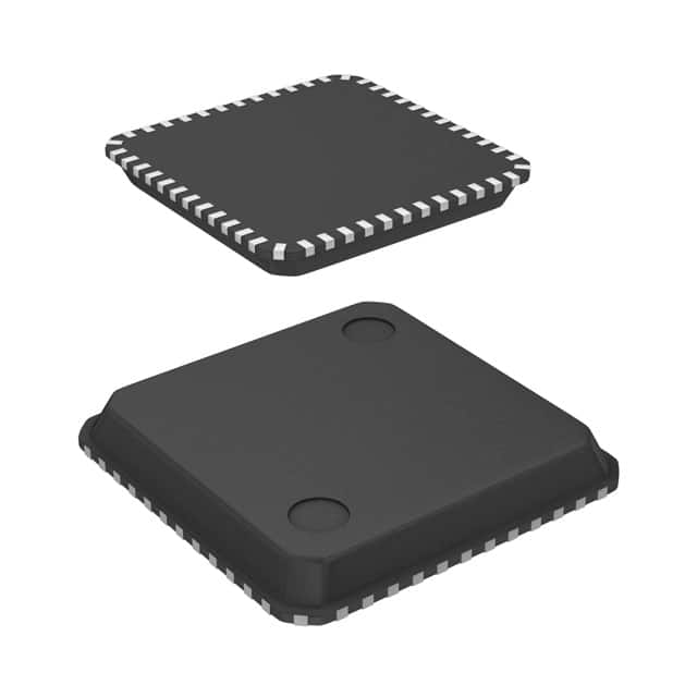
- Part No.:
- PEB 4262 V V1.1
- Manufacturer:
- Infineon Technologies
- Category:
- Telecom
- Package:
- 48-VFQFN Exposed Pad
- Datasheet:
-
 PEB 4262 V V1.1.pdf
- Description:
- IC TELECOM INTERFACE VQFN-48
- Quantity:
- Payment:

- Shipping:

Inventory:4,707
Please send an inquiry. Send us your inquiry, and we will respond immediately.
Product details
Overview
PEB 4262 V V1.1 from Infineon Technologies is a single-chip ISDN S/T interface transceiver IC designed for NT/TE boundary applications in digital telephony systems. It integrates line interface, codec, D-channel controller, and B-channel HDLC processors, supports 2B+D operation at 144 kbps, features integrated 2.048 MHz clock generation, and operates from a single 3.3 V supply.
For engineers reviewing the PEB 4262 V V1.1 datasheet, PEB 4262 V V1.1 pinout, PEB 4262 V V1.1 application, or PEB 4262 V V1.1 equivalent, key selection criteria include ISDN physical layer compliance (ETSI TS 101 524), integrated B-channel framing, on-chip PLL stability over temperature, and support for both point-to-point and point-to-multipoint S/T configurations.
Technical Context
The PEB 4262 V V1.1 implements full-duplex S/T interface functionality per ETSI EN 300 175-1 and ITU-T I.430, with integrated analog front-end including line driver, receiver, echo canceller, and adaptive equalizer. It embeds two independent B-channel HDLC controllers with automatic frame alignment and CRC-16 checking, plus a D-channel controller supporting LAPD protocol stack layers 1–2.
Its internal architecture includes a programmable 2.048 MHz oscillator with ±50 ppm accuracy, configurable gain control for transmit/receive paths, and hardware-based D-channel message buffering with 128-byte FIFO. All timing and synchronization are derived from the internal PLL locked to the incoming line clock or local crystal reference.
Key Specifications
| Parameter | Value and Actual Design Meaning |
|---|---|
| Interface Standard | ETSI EN 300 175-1 / ITU-T I.430 compliant S/T physical layer |
| Data Rate | 2×64 kbps B-channels + 16 kbps D-channel = 144 kbps aggregate |
| Supply Voltage | 3.3 V ±0.3 V - enables direct interfacing with 3.3 V logic without level shifters |
| Integrated Clock | 2.048 MHz oscillator with ±50 ppm tolerance - eliminates external crystal requirement |
| Operating Temp | −40 °C to +85 °C - qualified for industrial-grade telecom equipment deployment |
| Package | VQFN-48 (7 mm × 7 mm, 0.5 mm pitch) - supports high-density PCB layout with thermal pad |
Pinout & Package
VQFN-48 package with exposed thermal pad (EP), 0.5 mm pitch, 7 mm × 7 mm body size, RoHS-compliant lead-free finish.
| Pin/Terminal | Circuit Role | Design Meaning |
|---|---|---|
| TXP/TXN | Differential transmit output | Drives S/T line with ETSI-specified voltage swing and rise/fall times |
| RXP/RXN | Differential receive input | Accepts line signals with built-in echo cancellation and adaptive equalization |
| CLKOUT | 2.048 MHz clock output | Provides synchronous timing reference for external microcontroller or FPGA |
| RESETN | Active-low reset input | Asynchronous hardware reset with internal pull-up; initiates full state machine reinitialization |
| INTN | Interrupt request output | Open-drain signal indicating D-channel event, B-channel activity, or error condition |
Key Features
| Feature | Design Value |
|---|---|
| Integrated S/T line interface | Eliminates need for external line transformer, hybrid, and discrete amplifier components |
| On-chip D-channel controller | Handles LAPD layer-1 framing and layer-2 message sequencing without host CPU intervention |
| B-channel HDLC processing | Performs bit stuffing, CRC-16 calculation, and frame synchronization in hardware |
| Programmable gain control | Adjusts TX amplitude and RX sensitivity via SPI register writes to match line impedance variations |
Applications
| ISDN Terminal Adapter | VoIP Gateway Front-End |
|---|---|
Use Scenario: Standalone device converting analog phone lines or USB/Ethernet interfaces to ISDN S/T interface. IC Role / Device Role / Timing Role: Primary S/T physical layer transceiver and protocol engine handling all layer-1 and layer-2 signaling. Use Value: Reduces BOM count by integrating line driver, codec, and D-channel controller - cuts PCB area by >40% vs. discrete solution. | Use Scenario: Embedded module in enterprise VoIP gateway connecting PSTN trunk to IP network. IC Role / Device Role / Timing Role: Provides synchronized 2.048 MHz clock and B/D channel framing for TDM-to-packet conversion ASIC. Use Value: Enables deterministic jitter performance (<10 ns RMS) critical for voice packet timing alignment across multiple channels. |
| ISDN PBX Interface Card | Remote Access Server (RAS) |
Use Scenario: Line card in digital business telephone system supporting up to 30 concurrent ISDN lines. IC Role / Device Role / Timing Role: S/T interface per port with independent D-channel arbitration and B-channel multiplexing control. Use Value: Supports hot-plug detection and line fault reporting via dedicated status registers accessible over SPI. | Use Scenario: Dial-in concentrator providing secure remote LAN access via ISDN B-channels. IC Role / Device Role / Timing Role: Manages D-channel call setup/teardown and B-channel data path handoff to encryption processor. Use Value: Hardware-accelerated LAPD message parsing reduces host CPU load by ~35% during peak call setup traffic. |
Equivalent & Alternatives
The following parts are listed as comparable options for similar ISDN S/T interface applications.
| Alternative Part | Technical Difference | Application Difference | Selection Advice |
|---|---|---|---|
| Si2062-A-GM (Silicon Labs) | Requires external 2.048 MHz crystal; lacks integrated echo canceller; supports only point-to-point topology | No native support for multi-drop S/T bus configurations or D-channel broadcast addressing | Preferred where cost-sensitive designs can accommodate external clock and simplified line topology |
| ST72620J2 (STMicroelectronics) | Legacy 5 V operation; separate B/D channel control logic; no integrated PLL or clock generator | Needs level-shifting for 3.3 V host MCU; higher power consumption (120 mW vs. 85 mW) | Suitable for legacy board refreshes retaining existing 5 V power rails and discrete clock sources |
Compared with Si2062-A-GM and ST72620J2, the PEB 4262 V V1.1 delivers lower system-level component count through integrated clock, echo cancellation, and multi-topology support - reducing design validation effort and improving timing margin robustness in noise-prone telco environments.
Availability
PEB 4262 V V1.1 is available at Aetrix Electronics and suitable for ISDN terminal adapters, VoIP gateways, PBX interface cards, and remote access servers requiring stable component supply and long-term industrial lifecycle support.
Supply support for PEB 4262 V V1.1 includes scheduled delivery planning, volume procurement assistance, BOM continuity management, traceable sourcing, and lifecycle availability coordination for OEM customers, industrial embedded developers, connected-device designers, and electronics production programs.
Manufacturer
Infineon Technologies is a German semiconductor manufacturer specializing in power management, automotive, industrial, and communications ICs, with global R&D and manufacturing infrastructure.
The PEB 4262 V V1.1 belongs to Infineon's legacy Telecom Interface product line, engineered specifically for ETSI/ITU-T compliant ISDN S/T boundary implementations in carrier-class and enterprise telephony equipment.
FAQ
What is the maximum ambient temperature rating for continuous operation of the PEB 4262 V V1.1?
The PEB 4262 V V1.1 is rated for continuous operation from −40 °C to +85 °C ambient temperature, validated per JEDEC JESD22-A104 reliability testing. Thermal performance assumes proper PCB copper pour under the exposed pad and ≤2.5 W total power dissipation across all operating modes.
Does the PEB 4262 V V1.1 support both TE and NT mode operation?
Yes - the PEB 4262 V V1.1 supports configurable TE/NT mode selection via the MODE pin and internal register settings. In NT mode, it provides line termination, clock recovery, and D-channel master arbitration; in TE mode, it acts as a slave endpoint with line driving capability.
Can the integrated 2.048 MHz oscillator be bypassed for external clock injection?
Yes - the oscillator can be disabled using the CLKSEL bit in the CONFIG register, allowing external 2.048 MHz clock injection at the CLKIN pin. This mode maintains full timing synchronization and supports phase-locked operation when driven by a system-wide master clock source.
Is SPI the only host interface supported for configuration and status readback?
Yes - the PEB 4262 V V1.1 uses a 4-wire SPI interface (SCLK, MOSI, MISO, CSN) for all register access, firmware updates, and real-time status monitoring. No I²C, UART, or parallel interface options are implemented or supported in this revision.
PEB 4262 V V1.1 Specifications
- Product attributes
- Attribute value
- Manufacturer:
- Infineon Technologies
- Series:
- -
- Package/Case:
- 48-VFQFN Exposed Pad
- Packaging:
- Tape & Reel (TR)
- Product Status:
- Obsolete
- Function:
- Subscriber Line Interface Concept (SLIC)
- Interface:
- IOM-2, PCM
- Number of Circuits:
- 1
- Voltage - Supply:
- -
- Current - Supply:
- -
- Power (Watts):
- -
- Operating Temperature:
- 0°C ~ 70°C
- Grade:
- -
- Qualification:
- -
- Mounting Type:
- Surface Mount
- Supplier Device Package:
- PG-VQFN-48-4
PEB 4262 V V1.1 FAQ
1.How can I place an order for PEB 4262 V V1.1 through Aetrix?
Please submit a Request for Quotation (RFQ) for PEB 4262 V V1.1 on Aetrix. Our sales agent will provide a competitive quotation and guide you through the order confirmation once you accept the terms.
2.Are the price and stock information for PEB 4262 V V1.1 reliable?
The price and inventory of PEB 4262 V V1.1 are updated periodically and may fluctuate due to market conditions. Stock and pricing data are typically refreshed every 24 hours. Quotation validity for PEB 4262 V V1.1 is usually 5 days.
3.What payment methods are accepted for PEB 4262 V V1.1?
We accept Wire Transfer, PayPal, Credit Card, Western Union, MoneyGram, and Escrow for PEB 4262 V V1.1 transactions.
Note: Certain payment methods may incur a processing fee.
4.How is shipping managed for PEB 4262 V V1.1?
PEB 4262 V V1.1 orders can be shipped via leading logistics carriers, including DHL, UPS, FedEx, TNT, or Registered Mail.
Once your PEB 4262 V V1.1 order is processed, you will receive an email with the shipment details and tracking number.
Note: Tracking information may take up to 24 hours to appear. Express delivery typically takes 3–5 business days.
5.How can I obtain technical support or documentation for PEB 4262 V V1.1?
For technical support, including PEB 4262 V V1.1 datasheets, pinout diagrams, or application guidance, please contact our engineering support team. They can provide detailed documentation and assistance for your PEB 4262 V V1.1 requirements.
6.How does Aetrix verify that PEB 4262 V V1.1 is sourced from the original manufacturer or authorized distributors?
All PEB 4262 V V1.1 products on Aetrix are procured from qualified distributors and authorized channels. Our dedicated quality assurance team conducts strict verification, including traceability checks and, if necessary, third-party testing. This ensures that PEB 4262 V V1.1 meets industry standards.
7.What is the process for return or replacement of PEB 4262 V V1.1?
All PEB 4262 V V1.1 units undergo pre-shipment inspection (PSI). If there is an issue with PEB 4262 V V1.1, returns or replacements are accepted under the following conditions:
1.Quantity discrepancies, incorrect items, or visible external defects (such as breakage or corrosion), acknowledged by Aetrix.
2.The issue is reported within 90 days of delivery.
3.The PEB 4262 V V1.1 part is unused and in its original packaging.
Return procedure for PEB 4262 V V1.1:
1.Submit a request within 90 days.
2.Obtain a Return Material Authorization (RMA) from Aetrix.
PEB 4262 V V1.1 Tags

-
LMC567CMX/NOPB
Texas Instruments
-
LM567CMX/NOPB
Texas Instruments
-
LM567CM/NOPB
Texas Instruments

-
VSC8531XMW-02
Microchip Technology
-
VSC8531XMW-05
Microchip Technology

-
GPY115C0VI
MaxLinear, Inc.

-
SI32185-A-FMR
Skyworks Solutions Inc.

-
VSC8541XMV-05
Microchip Technology

-
SI32178-B-FM1R
Skyworks Solutions Inc.
-
GPY215C0VI
MaxLinear, Inc.

-
CPC7514ZTR
Littelfuse Inc.

-
VSC8502XML-03
Microchip Technology
Tech Hub

An engineering guide to LED driver operation, constant-current and constant-voltage outputs, linear and switching topologies, dimming, IC selection, calculations, replacement compatibility, and fault c…

Operational amplifier guide covering op amp basics, feedback, ideal vs real op amps, common configurations, buffer circuits, offset, bias current, gain-bandwidth, slew rate, rail-to-rail limits and sel…

Jumper cables guide covering safe connection order, red and black clamp placement, final ground connection, cable gauge, length, clamp quality, copper vs CCA cables, jump starter comparison and battery…

LDO regulator guide covering low dropout voltage, power dissipation, thermal design, PSRR, output noise, capacitor stability, adjustable LDO circuits, LDO vs buck converter and datasheet selection chec…

Conditional Access Module guide covering CAM meaning, CI/CI+ interface, smart card authorization, DVB security workflow, TV and set-top box compatibility, internal electronics, ESD protection, connecto…

Guide to electronic component obsolescence covering EOL risk, PCN/PDN notices, last-time buy planning, replacement options, form-fit-function validation, counterfeit risk and BOM lifecycle management.

18650 battery guide covering lithium-ion cell basics, 3.6V/3.7V voltage, 4.2V charging, mAh and Wh capacity, protected cells, chargers, BMS, series-parallel packs, holders, welding and sourcing checks.…

Hall effect sensor guide covering working principle, linear and digital sensors, Arduino circuits, current sensing, speed detection, automotive applications, A3144 examples, signal filtering and datash…

Product Change Notification guide for electronic components, covering PCN meaning, PCN vs PDN/EOL, common change types, risk levels, form-fit-function review, engineering validation, BOM control, LTB/L…

A practical guide to blend door actuators, covering HVAC function, symptoms, location, AC and heater issues, reset and calibration, replacement cost, electrical diagnosis, compatibility checks, and rep…


