
 My Inquiry
 My Account


Diodes Incorporated PI3EQX1002B1ZLEX
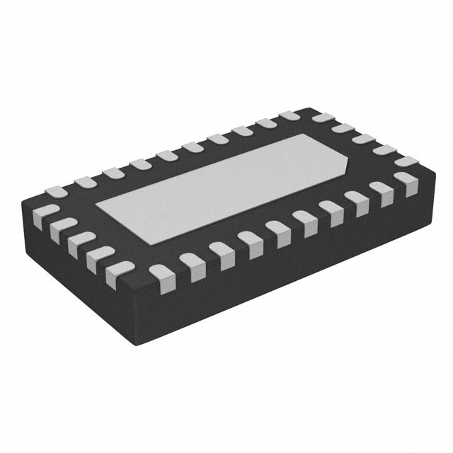
- Part No.:
- PI3EQX1002B1ZLEX
- Manufacturer:
- Diodes Incorporated
- Category:
- Signal Buffers, Repeaters, Splitters
- Package:
- 30-WFQFN Exposed Pad
- Datasheet:
-
 PI3EQX1002B1ZLEX.pdf
- Description:
- USB3 EQX W-QFN2545-30
- Quantity:
- Payment:

- Shipping:

Inventory:6,344
Please send an inquiry. Send us your inquiry, and we will respond immediately.
Product details
Overview
PI3EQX1002B1ZLEX from Diodes Incorporated is a 10.0 Gbps dual-channel linear ReDriver™ IC designed for USB 3.1 Gen-2 protocol extension, featuring programmable equalization (up to 14.6 dB at 5 GHz), flat gain (−1.6 to +2.7 dB), and output swing (800–1200 mVppd), operating on a single 3.3 V supply with automatic receiver detection and adaptive slumber mode for power-sensitive notebooks and docking stations.
For engineers reviewing the PI3EQX1002B1ZLEX datasheet, PI3EQX1002B1ZLEX pinout, PI3EQX1002B1ZLEX application, or PI3EQX1002B1ZLEX equivalent, this device supports high-fidelity signal integrity restoration across PCB traces, cables, and connectors in USB 3.1 host/device interconnects - with real-time channel-level power state management, CML I/O compatibility, and industrial temperature operation (−40°C to +85°C).
Technical Context
The PI3EQX1002B1 implements independent linear equalization per channel using analog DC-coupled compensation, supporting four discrete EQ settings (0/R/F/1) with frequency-dependent peaking gain up to 14.6 dB at 5 GHz. Each channel features fully autonomous input-level detection that triggers mode transitions between Active, Slumber (16–19 mA), Deep Slumber (0.4–0.6 mA), Unplug (0.3–0.45 mA), and Power-Down (<50 µA).
Its control architecture uses three 4-level pins per channel (EQA/B, FGA/B, SWA/B) with internal resistor dividers enabling hardware-selectable configuration without I²C or firmware. The integrated RXDET_EN and EN pins provide external enable/disable of receiver detection and full channel shutdown, while CML I/Os maintain 100 Ω differential impedance and support AC-coupled termination options including 50 Ω to VDD, 6 kΩ to VbiasTx, or Hi-Z.
Key Specifications
| Parameter | Value and Actual Design Meaning |
|---|---|
| Max Data Rate | 10.0 Gbps per channel - supports full USB 3.1 Gen-2 SuperSpeed signaling with <0.646 UI eye opening at silicon pad. |
| Equalization Range | 6.7–14.6 dB @2.5 GHz / 12.4–14.6 dB @5 GHz - selectable via EQA/B pins to compensate trace loss in long or lossy interconnects. |
| Flat Gain Control | −1.6 to +2.7 dB - adjustable via FGA/B pins to optimize signal amplitude before downstream receivers. |
| Output Swing | 800–1200 mVppd - configurable via SWA/B pins to match receiver sensitivity and reduce jitter-induced BER degradation. |
| Supply Voltage | 3.0–3.6 V - single 3.3 V rail operation with tight tolerance ensures stable biasing of CML output stages. |
| Operating Temp | −40°C to +85°C - qualified for industrial-grade embedded systems including docking stations and portable peripherals. |
| Power Modes | Active (130–167 mA), Slumber (16–19 mA), Deep Slumber (0.4–0.6 mA), Unplug (0.3–0.45 mA), Power Down (<50 µA) - enables dynamic power scaling per channel based on link activity. |
Pinout & Package
Package: 30-pin TQFN (2.5 mm × 4.5 mm, ZL30 footprint), thermally enhanced with exposed center pad requiring ≥3 thermal vias to GND plane.
| Pin/Terminal | Circuit Role | Design Meaning |
|---|---|---|
| VDD (Pins 1,10,16,25) | Power supply input | 3.3 V ±0.3 V supply for analog and digital circuitry; each pin must be decoupled with 0.1 µF capacitor near pad. |
| GND (Pins 4,5,6,7,13,19,20,21,22,28,Center Pad) | Ground reference | Low-inductance return path for all channels; center pad requires ≥3 thermal vias for thermal dissipation and EMI control. |
| EQA/EQB (Pins 26,15) | Equalization selection | 4-level analog control inputs (tie to GND/VDD/68kΩ/float) setting channel-specific EQ gain profile for loss compensation. |
| FGA/FGB (Pins 27,14) | Flat gain selection | 4-level analog control inputs configuring DC gain offset (−1.6 to +2.7 dB) to align output amplitude with receiver thresholds. |
| SWA/SWB (Pins 29,12) | Output swing selection | 4-level analog control inputs adjusting linear output swing (800–1200 mVppd) to minimize jitter and maximize eye margin. |
| AIP/AIN, BIP/BIN (Pins 2,3,17,18) | Differential CML inputs | 100 Ω differential CML receivers with selectable input termination (50 Ω to VDD, 67 kΩ to VbiasRx/GND) for flexible interface matching. |
| AOP/AON, BOP/BON (Pins 24,23,9,8) | Differential CML outputs | 100 Ω differential CML drivers with programmable output termination (50 Ω to VDD, 6 kΩ to VbiasTx, or Hi-Z) for cable/trace drive optimization. |
| RXDET_EN (Pin 11) | Receiver detection enable | Active-high logic input enabling/disabling automatic load presence sensing; internal 300 kΩ pull-up defaults to enabled. |
| EN (Pin 30) | Channel enable | Active-high logic input disabling entire channel (input/output buffers, EQ, swing circuits); internal 300 kΩ pull-up defaults to enabled. |
Key Features
| Feature | Design Value |
|---|---|
| Per-channel adaptive power management | Independent transition between Active, Slumber, Deep Slumber, Unplug, and Power-Down modes based on real-time input signal presence and duration. |
| Hardware-programmable signal conditioning | Three 4-level control pins per channel (EQ/FG/SW) allow full analog tuning of equalization, flat gain, and output swing without serial interface or firmware overhead. |
| USB 3.1 Gen-2 compliance | Fully compliant with USB 3.1 SuperSpeed electrical specifications including eye diagram, jitter, and common-mode voltage limits at 10 Gbps. |
| Automatic receiver detection | Integrated loop monitors input for LFPS patterns; re-enables detection after 7.3 ms idle time and enters Unplug Mode if no load is sensed. |
| Industrial-grade reliability | Qualified for −40°C to +85°C operation, RoHS 3/lead-free/halogen-free, and rated for 1.0 W continuous power dissipation in TQFN package. |
Applications
| USB 3.1 Docking Station | High-Density Notebook Expansion |
|---|---|
|
Use Scenario: Extending USB 3.1 Gen-2 signals from laptop motherboard to multi-port docking station with HDMI, DisplayPort, and SATA interfaces over 8+ layer PCBs. IC Role / Device Role / Timing Role: Linear ReDriver restoring signal integrity across lossy FR4 traces and connector transitions, compensating up to 15 dB insertion loss at 5 GHz. Use Value: Enables reliable 10 Gbps operation over >15 cm internal routing while maintaining USB-IF compliance and reducing bit error rate below 1e−12. |
Use Scenario: Signal boosting between USB controller and Type-C port in ultra-thin notebooks where trace length and layer count constrain signal fidelity. IC Role / Device Role / Timing Role: Dual-channel redriving with independent EQ/FG/SW tuning per lane to match asymmetric routing paths and connector losses. Use Value: Eliminates need for costly high-speed PCB materials by restoring eye opening to >0.625 UI at 5 Gbps and >0.646 UI at 10 Gbps per channel. |
| External SSD Enclosure | USB-C Monitor Hub |
|
Use Scenario: Driving USB 3.1 signals from host controller through EMI-shielded flex cable to NVMe SSD module inside aluminum enclosure. IC Role / Device Role / Timing Role: CML-to-CML redriver with AC-coupled outputs and programmable swing to overcome cable attenuation and connector reflections. Use Value: Maintains deterministic jitter <0.17 UI at 10 Gbps and supports hot-plug detection via RXDET_EN without host-side software intervention. |
Use Scenario: Signal regeneration in USB-C monitor hubs supporting simultaneous video (DP Alt Mode), data (USB 3.1), and power delivery over single cable. IC Role / Device Role / Timing Role: Isolated channel redriving with slumber mode activation during DP-only or idle states to reduce system standby power. Use Value: Lowers active current to 16–19 mA per channel in Slumber Mode and drops to <0.5 mA in Deep Slumber, extending battery life in portable displays. |
Equivalent & Alternatives
The following parts are listed as comparable options for similar USB 3.1 linear redriver applications.
| Alternative Part | Technical Difference | Application Difference | Selection Advice |
|---|---|---|---|
| TI TUSB211IRWBR | Single-channel, 5 Gbps USB 3.0 redriver with fixed EQ and no slumber mode; 24-pin WQFN package. | Limited to USB 3.0 (5 Gbps) and lacks per-channel power gating; suitable only for cost-sensitive, non-Gen-2 designs. | Select when Gen-2 speed and adaptive power are not required; avoid for 10 Gbps or battery-powered applications. |
| Renesas uPD720210 | USB 3.0 host controller with integrated redriver functionality; PCIe-based, requires driver stack and host CPU resources. | Not a standalone redriver - adds complexity, latency, and software dependency; unsuitable for transparent signal extension. | Choose only when adding USB host capability is primary goal; not a drop-in replacement for passive signal conditioning. |
Compared with TI TUSB211IRWBR and Renesas uPD720210, the PI3EQX1002B1ZLEX delivers true 10 Gbps Gen-2 performance with hardware-tunable EQ/FG/SW, autonomous per-channel power states, and minimal integration overhead - making it uniquely suited for low-latency, low-power, and layout-constrained USB 3.1 interconnects.
Availability
PI3EQX1002B1ZLEX is available at Aetrix Electronics and suitable for USB 3.1 docking stations, high-density notebook expansion modules, and external SSD enclosures requiring stable component supply, consistent lead-time visibility, and long-term lifecycle support.
Supply support for PI3EQX1002B1ZLEX includes scheduled delivery planning, volume procurement assistance, BOM continuity management, traceable sourcing, and lifecycle availability coordination for OEM customers, industrial embedded developers, connected-device designers, and electronics production programs.
Manufacturer
Diodes Incorporated is a global semiconductor company specializing in discrete, analog, and mixed-signal ICs, with design centers across Asia, Europe, and the U.S., serving industrial, computing, consumer, and communications markets.
The PI3EQX1002B1 belongs to Diodes' Pericom-branded high-speed interface portfolio, engineered specifically for USB, PCIe, and DisplayPort signal integrity enhancement in space- and power-constrained platforms.
FAQ
What is the function of the RXDET_EN pin?
RXDET_EN is an active-high enable input for the automatic receiver detection loop. When asserted (logic high), the device monitors input channels for LFPS patterns to detect attached loads; when deasserted (logic low), detection is disabled and the channel remains in its current power state. Internal 300 kΩ pull-up ensures default enable unless externally pulled low.
Can EQA and EQB be configured independently?
Yes - EQA controls Channel A equalization and EQB controls Channel B, with no coupling between them. Each accepts four distinct configurations (0/R/F/1) via external resistor ties or open-circuit, allowing asymmetric compensation for mismatched trace lengths or loss profiles in dual-lane USB 3.1 links.
What is the minimum input signal level required to exit Slumber Mode?
A minimum differential input amplitude of 45 mVppd (typical) at the AIP/AIN or BIP/BIN terminals is required to trigger wake-up from Slumber Mode. This threshold is defined by Vth_am in the datasheet and applies independently per channel when RXDET_EN is enabled.
Does the PI3EQX1002B1ZLEX support AC-coupled inputs and outputs?
Yes - both inputs (AIP/AIN, BIP/BIN) and outputs (AOP/AON, BOP/BON) are designed for AC-coupled operation with 75–265 nF recommended coupling capacitance. Input termination options include 50 Ω to VDD, 67 kΩ to VbiasRx/GND; output options include 50 Ω to VDD, 6 kΩ to VbiasTx, or Hi-Z.
PI3EQX1002B1ZLEX Specifications
- Product attributes
- Attribute value
- Manufacturer:
- Diodes Incorporated
- Series:
- ReDriver™
- Package/Case:
- 30-WFQFN Exposed Pad
- Packaging:
- Tape & Reel (TR)
- Product Status:
- Active
- Type:
- Buffer, ReDriver
- Applications:
- USB 3.1
- Input:
- CML
- Output:
- CML
- Data Rate (Max):
- 10Gbps
- Number of Channels:
- 1
- Delay Time:
- 2.0ns
- Signal Conditioning:
- Input Equalization
- Capacitance - Input:
- -
- Voltage - Supply:
- 3V ~ 3.6V
- Current - Supply:
- -
- Operating Temperature:
- 0°C ~ 70°C
- Grade:
- -
- Qualification:
- -
- Mounting Type:
- Surface Mount
- Supplier Device Package:
- 30-TQFN (2.5x4.5)
PI3EQX1002B1ZLEX FAQ
1.How can I place an order for PI3EQX1002B1ZLEX through Aetrix?
Please submit a Request for Quotation (RFQ) for PI3EQX1002B1ZLEX on Aetrix. Our sales agent will provide a competitive quotation and guide you through the order confirmation once you accept the terms.
2.Are the price and stock information for PI3EQX1002B1ZLEX reliable?
The price and inventory of PI3EQX1002B1ZLEX are updated periodically and may fluctuate due to market conditions. Stock and pricing data are typically refreshed every 24 hours. Quotation validity for PI3EQX1002B1ZLEX is usually 5 days.
3.What payment methods are accepted for PI3EQX1002B1ZLEX?
We accept Wire Transfer, PayPal, Credit Card, Western Union, MoneyGram, and Escrow for PI3EQX1002B1ZLEX transactions.
Note: Certain payment methods may incur a processing fee.
4.How is shipping managed for PI3EQX1002B1ZLEX?
PI3EQX1002B1ZLEX orders can be shipped via leading logistics carriers, including DHL, UPS, FedEx, TNT, or Registered Mail.
Once your PI3EQX1002B1ZLEX order is processed, you will receive an email with the shipment details and tracking number.
Note: Tracking information may take up to 24 hours to appear. Express delivery typically takes 3–5 business days.
5.How can I obtain technical support or documentation for PI3EQX1002B1ZLEX?
For technical support, including PI3EQX1002B1ZLEX datasheets, pinout diagrams, or application guidance, please contact our engineering support team. They can provide detailed documentation and assistance for your PI3EQX1002B1ZLEX requirements.
6.How does Aetrix verify that PI3EQX1002B1ZLEX is sourced from the original manufacturer or authorized distributors?
All PI3EQX1002B1ZLEX products on Aetrix are procured from qualified distributors and authorized channels. Our dedicated quality assurance team conducts strict verification, including traceability checks and, if necessary, third-party testing. This ensures that PI3EQX1002B1ZLEX meets industry standards.
7.What is the process for return or replacement of PI3EQX1002B1ZLEX?
All PI3EQX1002B1ZLEX units undergo pre-shipment inspection (PSI). If there is an issue with PI3EQX1002B1ZLEX, returns or replacements are accepted under the following conditions:
1.Quantity discrepancies, incorrect items, or visible external defects (such as breakage or corrosion), acknowledged by Aetrix.
2.The issue is reported within 90 days of delivery.
3.The PI3EQX1002B1ZLEX part is unused and in its original packaging.
Return procedure for PI3EQX1002B1ZLEX:
1.Submit a request within 90 days.
2.Obtain a Return Material Authorization (RMA) from Aetrix.
PI3EQX1002B1ZLEX Tags
-
PCA9509GM,125
NXP USA Inc.

-
PCA9617ADPJ
NXP USA Inc.

-
TCA9509DGKR
Texas Instruments

-
PCA9617ATPZ
NXP USA Inc.
-
PCA9517ADP,118
NXP USA Inc.
-
PCA9515ADP,118
NXP USA Inc.
-
PCA9515AD,118
NXP USA Inc.
-
PCA9517DP,118
NXP USA Inc.

-
TUSB211ARWBR
Texas Instruments
-
PCA9517AD,118
NXP USA Inc.
-
PCA9517ATP,147
NXP USA Inc.

-
P82B96PWR
Texas Instruments
Tech Hub

Operational amplifier guide covering op amp basics, feedback, ideal vs real op amps, common configurations, buffer circuits, offset, bias current, gain-bandwidth, slew rate, rail-to-rail limits and sel…

Jumper cables guide covering safe connection order, red and black clamp placement, final ground connection, cable gauge, length, clamp quality, copper vs CCA cables, jump starter comparison and battery…

LDO regulator guide covering low dropout voltage, power dissipation, thermal design, PSRR, output noise, capacitor stability, adjustable LDO circuits, LDO vs buck converter and datasheet selection chec…

Conditional Access Module guide covering CAM meaning, CI/CI+ interface, smart card authorization, DVB security workflow, TV and set-top box compatibility, internal electronics, ESD protection, connecto…

Guide to electronic component obsolescence covering EOL risk, PCN/PDN notices, last-time buy planning, replacement options, form-fit-function validation, counterfeit risk and BOM lifecycle management.

18650 battery guide covering lithium-ion cell basics, 3.6V/3.7V voltage, 4.2V charging, mAh and Wh capacity, protected cells, chargers, BMS, series-parallel packs, holders, welding and sourcing checks.…

Hall effect sensor guide covering working principle, linear and digital sensors, Arduino circuits, current sensing, speed detection, automotive applications, A3144 examples, signal filtering and datash…

Product Change Notification guide for electronic components, covering PCN meaning, PCN vs PDN/EOL, common change types, risk levels, form-fit-function review, engineering validation, BOM control, LTB/L…

A practical guide to blend door actuators, covering HVAC function, symptoms, location, AC and heater issues, reset and calibration, replacement cost, electrical diagnosis, compatibility checks, and rep…

Engineering guide to Raspberry Pi alternatives, covering chip-level differences, Orange Pi, ROCK, Jetson, Banana Pi, NanoPi, Compute Module, Pico, GPIO, camera, HAT compatibility, and replacement risks…


