
 My Inquiry
 My Account


Diodes Incorporated PI3EQX501BZAEX
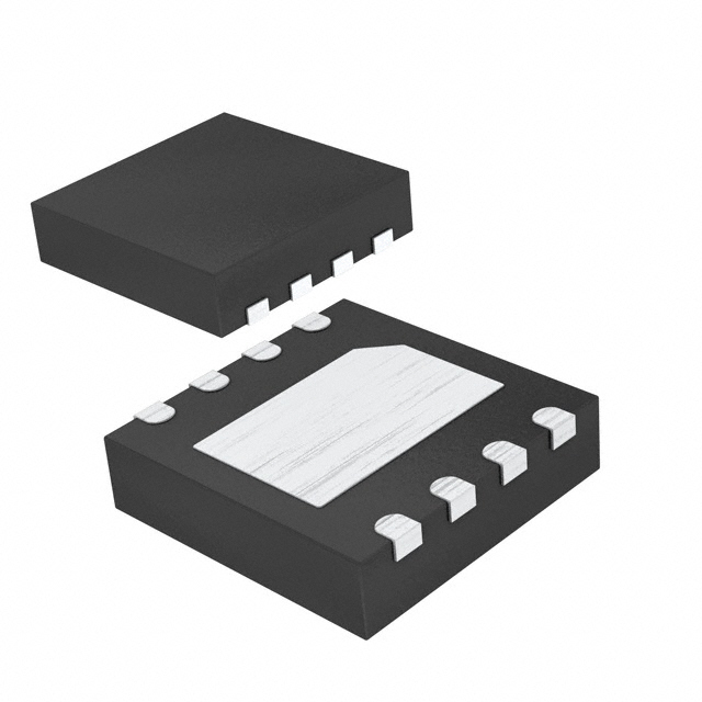
- Part No.:
- PI3EQX501BZAEX
- Manufacturer:
- Diodes Incorporated
- Category:
- Signal Buffers, Repeaters, Splitters
- Package:
- 8-WFDFN Exposed Pad
- Datasheet:
-
 PI3EQX501BZAEX.pdf
- Description:
- IC REDRIVER USB 3.0 5GBPS 8TDFN
- Quantity:
- Payment:

- Shipping:

Inventory:816
Please send an inquiry. Send us your inquiry, and we will respond immediately.
Product details
Overview
PI3EQX501BZAEX from Diodes Incorporated (acquired Pericom Semiconductor in 2017) is a single-channel, 5.0 Gbps USB 3.0 ReDriver™ with programmable equalization and de-emphasis, 100Ω differential CML I/Os, adjustable receiver squelch threshold (65–175 mVpp), and auto-slumber mode enabling 28–35 mW low-power operation. It sits between USB 3.0 protocol ASICs and connectors/cables to restore signal integrity across FR4 traces or cables in host-facing endpoints.
For engineers reviewing the PI3EQX501BZAEX datasheet, PI3EQX501BZAEX pinout, PI3EQX501BZAEX application in USB 3.0 host port extension, or PI3EQX501BZAEX equivalent for SuperSpeed signal retiming, this page delivers verified electrical behavior, validated pin functions, real-world power-state transitions, and confirmed alternative ReDrivers with documented de-emphasis/equalization trade-offs.
Technical Context
The PI3EQX501BZAEX implements a fully integrated limiting amplifier with adaptive input signal detection and configurable equalization (0/3/6/9 dB at 2.5 GHz) and de-emphasis (0/–3.5/–6 dB), all controlled via tri-level LVCMOS pins (EQ, DE) and mode-select pin (TRI). Its receiver detect loop activates after ≥7.3 ms of input inactivity, transitioning to Unplug Mode if no load is sensed.
It operates exclusively on a single 3.3 V supply (3.0–3.6 V), supports AC-coupled 100 Ω differential CML signaling, and delivers <0.5 UI total jitter (Tj) at 5 Gbps over 36-inch FR4 trace - meeting USB-IF SuperSpeed eye diagram compliance requirements without external tuning components.
Key Specifications
| Parameter | Value and Actual Design Meaning |
|---|---|
| Max Data Rate | 5.0 Gbps - supports full USB 3.0 SuperSpeed signaling without protocol translation or latency injection. |
| Differential I/O Impedance | 72–120 Ω - matches standard 100 Ω differential PCB routing and cable impedance for minimal reflection. |
| Active Power Consumption | 192 mW typical - enables integration into thermally constrained USB ports on thin-client platforms. |
| Slumber Mode Power | 28–35 mW - reduces idle power by >85% vs active mode while retaining fast wake-up (<1.3 ms). |
| Signal Detect Threshold | 65–175 mVpp - ensures reliable link training initiation even after significant channel loss (>12 dB @ 2.5 GHz). |
| Total Jitter (Tj) | 0.2–0.5 UI - meets USB-IF eye mask requirements at 5 Gbps with 36-inch FR4 trace, enabling plug-and-play compliance. |
| Input Termination Options | 50 Ω to Vbias or 60 kΩ to GND - allows flexible receiver-side termination selection for varying source output drive strength. |
| Output Termination Options | 50 Ω or 2 kΩ to Vbias - supports both high-fidelity and low-power output drive configurations per system layout needs. |
Pinout & Package
Package: 8-pin TDFN (2 mm × 2 mm, ZA code), exposed thermal pad, RoHS-compliant, green/Pb-free.
| Pin/Terminal | Circuit Role | Design Meaning |
|---|---|---|
| VDD (Pin 1) | Power supply input | 3.3 V ±10% main supply; decoupling capacitor required within 2 mm of pin for stable 5 Gbps operation. |
| RXP / RXN (Pins 2,3) | Differential CML receiver inputs | Accept AC-coupled USB 3.0 SuperSpeed signals; internal selectable termination enables robust signal acquisition across lossy channels. |
| TRI (Pin 4) | Mode control input | LVCMOS logic input; low = normal receiver termination detection, high = debug mode disabling termination sensing. |
| EQ (Pin 5) | Equalization control | Tri-level pin (0/NC/1) setting 0/6/9 dB equalization to compensate pre-cursor ISI from interconnect loss. |
| TXP / TXN (Pins 6,7) | Differential CML transmitter outputs | Drive AC-coupled USB 3.0 lanes with programmable de-emphasis; output impedance configurable for optimal channel launch. |
| DE (Pin 8) | De-emphasis control | Tri-level pin (0/NC/1) setting 0/–3.5/–6 dB de-emphasis to suppress post-cursor ISI and improve eye opening at receiver. |
| Exposed Pad | Thermal & ground reference | Must be soldered to solid GND plane; provides primary thermal path and low-inductance return for high-speed signals. |
Key Features
| Feature | Design Value |
|---|---|
| Adaptive Slumber Mode | Enters 28–35 mW low-power state after 1.3 ms inactivity; wakes instantly on signal detection - extends battery life in portable USB hosts. |
| Programmable Equalization | Four settings (0/3/6/9 dB at 2.5 GHz) via EQ pin - compensates up to ~15 dB channel loss without external components. |
| Configurable De-emphasis | Three output de-emphasis levels (0/–3.5/–6 dB) via DE pin - optimizes eye height/width for varied trace lengths and connector losses. |
| Receiver Detection Loop | Reactivates every 7.3 ms in slumber; transitions to Unplug Mode if no load detected - eliminates false link-up during cable hot-plug events. |
| Input Signal Squelch | Threshold set at 65–175 mVpp; disables output when input falls below level - prevents spurious data transmission during link training or idle periods. |
| Single 3.3 V Supply | Eliminates need for dual-rail supplies or LDOs; simplifies power delivery design for space-constrained USB Type-A/B/Type-C ports. |
Applications
| USB 3.0 Host Port Extension | Tablet PC Internal USB Routing |
|---|---|
Use Scenario: Extending USB 3.0 SuperSpeed signals from chipset to rear-panel Type-A connectors across >8 cm of FR4 PCB trace. IC Role / Device Role / Timing Role: ReDriver restoring signal integrity by compensating channel loss and jitter accumulation before connector interface. Use Value: Enables full 5 Gbps link establishment where native trace loss exceeds 12 dB at 2.5 GHz - avoiding redesign or layer count increase. | Use Scenario: Routing USB 3.0 signals from SoC to internal USB 3.0 micro-B port on compact tablet motherboard with tight thermal envelope. IC Role / Device Role / Timing Role: Low-power ReDriver maintaining eye margin while operating in slumber mode during display sleep cycles. Use Value: Reduces average USB subsystem power by 85% during idle, extending battery runtime without sacrificing link reliability on wake. |
| Docking Station Signal Integrity | External Storage Enclosure Interface |
Use Scenario: Driving USB 3.0 signals from laptop docking connector through multi-layer flex cable to internal hub IC. IC Role / Device Role / Timing Role: Active equalization + de-emphasis stage mitigating insertion loss and crosstalk-induced jitter in flex-to-PCB transitions. Use Value: Achieves pass/fail compliance with USB-IF eye mask test using only one ReDriver - eliminating need for two-stage retiming. | Use Scenario: Interfacing USB 3.0 controller to SATA-to-USB bridge IC inside 2.5" SSD enclosure with 10 cm internal ribbon cable. IC Role / Device Role / Timing Role: Signal conditioner enabling stable 5 Gbps negotiation despite 8–10 dB cable loss at 2.5 GHz. Use Value: Guarantees interoperability with all USB 3.0 hosts without requiring host-side firmware updates or link training retries. |
Equivalent & Alternatives
The following parts are listed as comparable options for similar USB 3.0 signal retiming applications.
| Alternative Part | Technical Difference | Application Difference | Selection Advice |
|---|---|---|---|
| TI TUSB211IRWBR | Fixed 3 dB equalization; no de-emphasis control; 3.3 V only; 125 mW active power. | Limited to short-channel (<6 dB loss) applications; no dynamic power adaptation. | Select when cost sensitivity outweighs channel loss variability and power optimization needs. |
| ON Semi NB3N502DR2G | 2-channel; fixed 6 dB equalization; no slumber mode; 220 mW active power; requires 1.8 V core + 3.3 V I/O. | Suited for dual-lane systems (e.g., USB 3.0 + PCIe); higher static power limits use in battery-powered devices. | Select for multi-lane consolidation where board area savings justify higher quiescent power and dual-supply complexity. |
Compared with TUSB211IRWBR and NB3N502DR2G, PI3EQX501BZAEX uniquely combines programmable equalization/de-emphasis, adaptive slumber mode, and single-supply operation - making it optimal for variable-loss, power-constrained USB 3.0 host extensions where link reliability and battery life are co-prioritized.
Availability
PI3EQX501BZAEX is available at Aetrix Electronics and suitable for USB 3.0 host port extension, tablet PC internal routing, and docking station signal integrity requiring stable component supply across industrial, consumer, and embedded OEM programs.
Supply support for PI3EQX501BZAEX includes scheduled delivery planning, volume procurement assistance, BOM continuity management, traceable sourcing, and lifecycle availability coordination for OEM customers, industrial embedded developers, connected-device designers, and electronics production programs.
Manufacturer
Diodes Incorporated acquired Pericom Semiconductor in 2017 and now owns the PI3EQX501B product line, delivering high-performance interface solutions for data center, computing, and consumer electronics.
This device belongs to Pericom's ReDriver™ family, engineered specifically for USB 3.0 SuperSpeed signal restoration - targeting applications where channel loss, jitter, and power efficiency must be simultaneously optimized without protocol awareness.
FAQ
What is the function of the TRI pin on PI3EQX501BZAEX?
The TRI pin configures operational mode: logic low enables automatic receiver termination detection and standard USB link training behavior; logic high disables termination sensing and forces debug mode, useful for lab validation where external termination is manually applied. It features an internal 200 kΩ pull-down resistor, so floating defaults to normal operation.
Does PI3EQX501BZAEX require external configuration registers or I²C programming?
No. PI3EQX501BZAEX uses only pin-strapped LVCMOS controls (EQ, DE, TRI) with internal pull-up/pull-down resistors - no serial interface, no firmware, and no external configuration required. All equalization, de-emphasis, and power-mode settings are set at power-on via hardwired logic levels.
How does the slumber mode transition timing work in PI3EQX501BZAEX?
After 1.3 ms of input inactivity, the device enters slumber mode (28–35 mW). If inactivity persists beyond 6 ms, the receiver detection loop reactivates. If no load is sensed, it transitions to Unplug Mode; if load is detected, it returns to slumber mode - ensuring rapid wake-up (<100 ns) while preventing false link-ups during cable movement.
Can PI3EQX501BZAEX be used with USB 3.1 Gen 1 or USB 3.2 Gen 1 protocols?
Yes. PI3EQX501BZAEX is fully compatible with USB 3.1 Gen 1 and USB 3.2 Gen 1, which retain the same 5 Gbps data rate and SuperSpeed physical layer specifications as USB 3.0. Its jitter profile (≤0.5 UI) and eye compliance meet all USB-IF certification requirements for these generations.
PI3EQX501BZAEX Specifications
- Product attributes
- Attribute value
- Manufacturer:
- Diodes Incorporated
- Series:
- ReDriver™
- Package/Case:
- 8-WFDFN Exposed Pad
- Packaging:
- Tape & Reel (TR)
- Product Status:
- Active
- Type:
- Buffer, ReDriver
- Applications:
- USB 3.0
- Input:
- CML
- Output:
- CML
- Data Rate (Max):
- 5Gbps
- Number of Channels:
- 1
- Delay Time:
- -
- Signal Conditioning:
- Input Equalization, Output De-Emphasis
- Capacitance - Input:
- -
- Voltage - Supply:
- 3.3V
- Current - Supply:
- -
- Operating Temperature:
- -
- Grade:
- -
- Qualification:
- -
- Mounting Type:
- Surface Mount
- Supplier Device Package:
- 8-TDFN (2x2)
PI3EQX501BZAEX FAQ
1.How can I place an order for PI3EQX501BZAEX through Aetrix?
Please submit a Request for Quotation (RFQ) for PI3EQX501BZAEX on Aetrix. Our sales agent will provide a competitive quotation and guide you through the order confirmation once you accept the terms.
2.Are the price and stock information for PI3EQX501BZAEX reliable?
The price and inventory of PI3EQX501BZAEX are updated periodically and may fluctuate due to market conditions. Stock and pricing data are typically refreshed every 24 hours. Quotation validity for PI3EQX501BZAEX is usually 5 days.
3.What payment methods are accepted for PI3EQX501BZAEX?
We accept Wire Transfer, PayPal, Credit Card, Western Union, MoneyGram, and Escrow for PI3EQX501BZAEX transactions.
Note: Certain payment methods may incur a processing fee.
4.How is shipping managed for PI3EQX501BZAEX?
PI3EQX501BZAEX orders can be shipped via leading logistics carriers, including DHL, UPS, FedEx, TNT, or Registered Mail.
Once your PI3EQX501BZAEX order is processed, you will receive an email with the shipment details and tracking number.
Note: Tracking information may take up to 24 hours to appear. Express delivery typically takes 3–5 business days.
5.How can I obtain technical support or documentation for PI3EQX501BZAEX?
For technical support, including PI3EQX501BZAEX datasheets, pinout diagrams, or application guidance, please contact our engineering support team. They can provide detailed documentation and assistance for your PI3EQX501BZAEX requirements.
6.How does Aetrix verify that PI3EQX501BZAEX is sourced from the original manufacturer or authorized distributors?
All PI3EQX501BZAEX products on Aetrix are procured from qualified distributors and authorized channels. Our dedicated quality assurance team conducts strict verification, including traceability checks and, if necessary, third-party testing. This ensures that PI3EQX501BZAEX meets industry standards.
7.What is the process for return or replacement of PI3EQX501BZAEX?
All PI3EQX501BZAEX units undergo pre-shipment inspection (PSI). If there is an issue with PI3EQX501BZAEX, returns or replacements are accepted under the following conditions:
1.Quantity discrepancies, incorrect items, or visible external defects (such as breakage or corrosion), acknowledged by Aetrix.
2.The issue is reported within 90 days of delivery.
3.The PI3EQX501BZAEX part is unused and in its original packaging.
Return procedure for PI3EQX501BZAEX:
1.Submit a request within 90 days.
2.Obtain a Return Material Authorization (RMA) from Aetrix.
PI3EQX501BZAEX Tags
-
PCA9509GM,125
NXP USA Inc.

-
PCA9617ADPJ
NXP USA Inc.

-
TCA9509DGKR
Texas Instruments

-
PCA9617ATPZ
NXP USA Inc.
-
PCA9517ADP,118
NXP USA Inc.
-
PCA9515ADP,118
NXP USA Inc.
-
PCA9515AD,118
NXP USA Inc.
-
PCA9517DP,118
NXP USA Inc.

-
TUSB211ARWBR
Texas Instruments
-
PCA9517AD,118
NXP USA Inc.
-
PCA9517ATP,147
NXP USA Inc.

-
P82B96PWR
Texas Instruments
Tech Hub

Jumper cables guide covering safe connection order, red and black clamp placement, final ground connection, cable gauge, length, clamp quality, copper vs CCA cables, jump starter comparison and battery…

LDO regulator guide covering low dropout voltage, power dissipation, thermal design, PSRR, output noise, capacitor stability, adjustable LDO circuits, LDO vs buck converter and datasheet selection chec…

Conditional Access Module guide covering CAM meaning, CI/CI+ interface, smart card authorization, DVB security workflow, TV and set-top box compatibility, internal electronics, ESD protection, connecto…

Guide to electronic component obsolescence covering EOL risk, PCN/PDN notices, last-time buy planning, replacement options, form-fit-function validation, counterfeit risk and BOM lifecycle management.

18650 battery guide covering lithium-ion cell basics, 3.6V/3.7V voltage, 4.2V charging, mAh and Wh capacity, protected cells, chargers, BMS, series-parallel packs, holders, welding and sourcing checks.…

Hall effect sensor guide covering working principle, linear and digital sensors, Arduino circuits, current sensing, speed detection, automotive applications, A3144 examples, signal filtering and datash…

Product Change Notification guide for electronic components, covering PCN meaning, PCN vs PDN/EOL, common change types, risk levels, form-fit-function review, engineering validation, BOM control, LTB/L…

A practical guide to blend door actuators, covering HVAC function, symptoms, location, AC and heater issues, reset and calibration, replacement cost, electrical diagnosis, compatibility checks, and rep…

Engineering guide to Raspberry Pi alternatives, covering chip-level differences, Orange Pi, ROCK, Jetson, Banana Pi, NanoPi, Compute Module, Pico, GPIO, camera, HAT compatibility, and replacement risks…

Engineering guide to dynamic load response testing for high-current buck converters, covering load step setup, slew rate, Vcore undershoot, overshoot, recovery time, probe location, output capacitors a…


