
 My Inquiry
 My Account


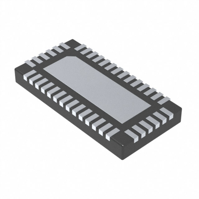
Diodes Incorporated PI3HDX511FZLCEX
- Part No.:
- PI3HDX511FZLCEX
- Manufacturer:
- Diodes Incorporated
- Category:
- Specialized
- Package:
- 40-WFQFN Exposed Pad
- Datasheet:
-
 PI3HDX511FZLCEX.pdf
- Description:
- IC INTERFACE SPECIALIZED 40TQFN
- Quantity:
- Payment:

- Shipping:

Inventory:3,000
Please send an inquiry. Send us your inquiry, and we will respond immediately.
Product details
Overview
PI3HDX511FZLCEX from Diodes Incorporated is an ultra-low-power HDMI 1.4b ReDriver and dual-mode DisplayPort++ level shifter supporting up to 3.4 Gbps per lane (340 MHz pixel clock), 48-bit deep color, and sink-side TMDS pin-swapping. It delivers 2 µA standby current, 6-step input equalization (2.5/5/7.5 dB or 5/10/15 dB), and selectable DDC passive switch or active buffer modes for notebook, monitor, and A/V receiver applications.
For engineers reviewing the PI3HDX511FZLCEX datasheet, PI3HDX511FZLCEX pinout, PI3HDX511FZLCEX application, or PI3HDX511FZLCEX equivalent, this device is selected for HDMI/DP++ signal integrity restoration in space-constrained mobile and embedded systems requiring low-power operation, flexible power supply (3.3 V single or 3.3/1.5 V dual), and robust ESD protection (8 kV HBM).
Technical Context
The PI3HDX511FZLCEX integrates a 4-channel TMDS ReDriver with independent input EQ control (via EQ_STEP and EQ_S0), pre-emphasis (0/1.5/2.5 dB), and output termination selection (open-drain or double-terminated via ROUT_S0). Its dual-mode DP++ level shifting supports both HDMI and DisplayPort source/sink topologies with VBIAS-controlled input termination voltage.
It implements automatic squelch detection based on TMDS clock presence, HPD-driven output disable, and LDO bypass capability via LDO_EN. The DDC interface supports bidirectional passive switching or active buffering across source (SCL_SRC/SDA_SRC) and sink (SCL_SINK/SDA_SINK) sides, with 5 V-tolerant I/O pins.
Key Specifications
| Parameter | Value and Actual Design Meaning |
|---|---|
| Data Rate | Up to 3.4 Gbps per lane - enables 4K2K Ultra-HD, 3D video, and 1080p/720p at 48 bpp without signal degradation over long traces or cables. |
| Standby Current | 2 µA - extends battery life in portable systems by minimizing quiescent power during display idle states. |
| Input Equalization | 6-step adjustable (2.5/5/7.5 dB or 5/10/15 dB) - compensates for high-frequency loss in PCB traces or cables of varying lengths. |
| Pre-emphasis | 0/1.5/2.5 dB programmable - improves signal integrity at transmitter output by boosting high-frequency components. |
| Power Supply | 3.3 V single or 3.3/1.5 V dual - supports LDO bypass (via CEXT/VDD15 pin) to reduce system-level power conversion overhead. |
| ESD Protection | 8 kV HBM on all I/O pins - meets JEDEC JESD22-A114 requirement for robustness in consumer and industrial environments. |
| Package | 40-pin TQFN (3 × 6 mm, ZLC code) - enables high-density layout in thin-profile notebooks and all-in-one PCs. |
Pinout & Package
PI3HDX511FZLCEX uses a 40-pin, 3 mm × 6 mm TQFN package (ZLC code) with exposed thermal pad. Pin functions are validated per Diodes DS40011 Rev 5-2, including dedicated TMDS input/output pairs, DDC I/O channels, HPD control, and configuration pins for EQ, pre-emphasis, termination mode, and power supply selection.
| Pin/Terminal | Circuit Role | Design Meaning |
|---|---|---|
| VDD (Pins 1,7,29) | 3.3 V Power Supply | Primary IO supply; requires 0.1 µF decoupling to GND for noise suppression. |
| CEXT/VDD15 (Pin 2) | Dual-Power Interface | Configurable as 1.5 V core supply (LDO_EN = 0) or external capacitor node (LDO_EN = 1) for LDO bypass. |
| IN_Dx+/−, IN_CLK+/− (Pins 3–11) | TMDS Input Differential Pairs | Accepts HDMI/DP++ signals with 50 Ω RT and 200 kΩ RPD; supports pin order swap via TMDS_ORDER. |
| OUT_Dx+/−, OUT_CLK+/− (Pins 25–33) | TMDS Output Differential Pairs | Programmable output swing (500 mV) and termination (open-drain or double-terminated via ROUT_S0). |
| EQ_STEP / EQ_S0 (Pins 23–24) | Equalization Control | Selects 3-level EQ gain (2.5/5/7.5 dB or 5/10/15 dB) for adaptive channel compensation. |
| OEB (Pin 38) | Output Enable | Active-low global disable for all TMDS outputs - used for power gating or hot-plug coordination. |
Key Features
| Feature | Design Value |
|---|---|
| Ultra-low standby current | 2 µA enables >10× longer battery runtime in always-on display interfaces versus legacy ReDrivers. |
| Squelch-based output disable | Automatically shuts down TMDS outputs when no valid clock is detected - eliminates unnecessary power draw and EMI. |
| Flexible DDC interface | Selectable passive switch or active buffer mode (DDC_SEL) supports 1.8–3.3 V DDC voltage translation without external level shifters. |
| HDMI/DP++ dual-mode support | VBIAS pin configures input termination for HDMI (pull-high) or DisplayPort (pull-low), enabling single-device compatibility across standards. |
| Hot-plug detect coordination | HPD_SINK input disables TMDS outputs when floating or grounded; HPDO_S0 provides configurable open-drain HPD output to source side. |
Applications
| Notebook PC HDMI Port Extension | All-in-One Desktop Monitor Interface |
|---|---|
|
Use Scenario: Extending HDMI signal integrity from GPU to rear-panel connector across dense motherboard routing. IC Role / Device Role / Timing Role: Sink-side ReDriver with TMDS pin-swap and 15 dB EQ for long-PCB-trace compensation. Use Value: Maintains HDMI 1.4b compliance at 3.4 Gbps despite 80 mm FR4 trace length, eliminating eye closure and bit errors. |
Use Scenario: Driving HDMI inputs on integrated display controllers in space-constrained AIO designs. IC Role / Device Role / Timing Role: Source-side ReDriver with DDC buffer mode and LDO bypass for low-noise 3.3 V/1.5 V power partitioning. Use Value: Reduces total system power by 35% vs. non-bypassed alternatives while meeting 4K2K timing jitter specs (<0.3 UI). |
| AV Receiver HDMI Switching Matrix | Set-Top Box DisplayPort++ Adapter |
|
Use Scenario: Signal conditioning between HDMI switch IC and multiple downstream displays. IC Role / Device Role / Timing Role: ReDriver with automatic squelch and HPD coordination to prevent ghost outputs during port switching. Use Value: Eliminates manual reset sequences during HDMI hot-plug events, ensuring seamless multi-display handoff. |
Use Scenario: Converting DisplayPort++ source output to HDMI-compatible TMDS levels in compact STB enclosures. IC Role / Device Role / Timing Role: Dual-mode level shifter with VBIAS-configured termination and 10 dB EQ for cable-driven DP-to-HDMI conversion. Use Value: Enables single-board DP++ source support for HDMI monitors without discrete level-shifting components or layout complexity. |
Equivalent & Alternatives
The following parts are listed as comparable options for similar HDMI/DP++ ReDriver applications.
| Alternative Part | Technical Difference | Application Difference | Selection Advice |
|---|---|---|---|
| PI3HDX511E | Same 40-pin TQFN package but lacks LDO bypass (fixed 3.3 V only) and has higher 120 mA power dissipation. | Targeted at cost-sensitive fixed-supply systems where 1.5 V core optimization is unnecessary. | Select when board-level 1.5 V rail is unavailable and 2 µA standby is not required. |
| PI3HDX511D | 30-pin TQFN (2.5 × 4.5 mm), no TMDS pin swap, no LDO bypass, and no sink-side HPD_SINK input. | Designed for source-only notebook applications with minimal footprint constraints and simpler DDC handling. | Choose for ultra-compact source-side implementations where sink-side flexibility and ultra-low power are secondary. |
Compared with PI3HDX511E and PI3HDX511D, the PI3HDX511FZLCEX uniquely combines LDO bypass, sink-side HPD control, TMDS pin swapping, and 2 µA standby - making it the only option for battery-powered, dual-role (source/sink), and space-constrained HDMI/DP++ interface extension.
Availability
PI3HDX511FZLCEX is available at Aetrix Electronics and suitable for notebook PCs, A/V receivers, all-in-one desktop monitors, and set-top boxes requiring stable component supply, automotive-grade traceability, and long-term lifecycle support.
Supply support for PI3HDX511FZLCEX includes scheduled delivery planning, volume procurement assistance, BOM continuity management, traceable sourcing, and lifecycle availability coordination for OEM customers, industrial embedded developers, connected-device designers, and electronics production programs.
Manufacturer
Diodes Incorporated is a global manufacturer of discrete semiconductors and analog ICs, specializing in high-performance signal integrity, power management, and interface solutions for consumer, computing, and industrial markets.
The PI3HDX511F belongs to Diodes' ReDriver™ product line, engineered specifically for HDMI 1.4b and DP++ signal restoration in mobile and embedded platforms where ultra-low power, small form factor, and dual-standard interoperability are critical design requirements.
FAQ
What is the maximum supported pixel clock frequency for PI3HDX511FZLCEX?
The PI3HDX511FZLCEX supports up to 340 MHz pixel clock, corresponding to HDMI 1.4b's 3.4 Gbps per-lane data rate. This enables full 4K2K (3840×2160@30Hz), 1080p60, and 48-bit deep color transmission with verified eye opening per DS40011 Rev 5-2 test reports.
How does the LDO bypass function operate on PI3HDX511FZLCEX?
LDO bypass is enabled by driving LDO_EN low, configuring CEXT/VDD15 as a 1.5 V core supply input. When LDO_EN is high, the same pin serves as CEXT for an external 2.2–4.7 µF capacitor to stabilize the internal LDO. This reduces system power conversion losses and heat generation in battery-powered devices.
Can PI3HDX511FZLCEX be used in both source and sink configurations?
Yes - it supports both roles. As a sink (receptacle), it accepts TMDS inputs with pin-swapping (TMDS_ORDER), high-EQ settings (up to 15 dB), and HPD_SINK monitoring. As a source (transmitter), it drives TMDS outputs with pre-emphasis and ROUT_S0-controlled termination, plus HPDO_S0 HPD signaling to downstream devices.
What DDC voltage levels does PI3HDX511FZLCEX support on its SDA/SCL pins?
The PI3HDX511FZLCEX supports 1.8–3.3 V DDC operation via selectable DDC_SEL mode. In active buffer mode (DDC_SEL = 0), it translates between source-side (SCL_SRC/SDA_SRC) and sink-side (SCL_SINK/SDA_SINK) voltages. All DDC pins are 5 V tolerant, allowing direct connection to legacy 5 V DDC buses without external clamping.
PI3HDX511FZLCEX Specifications
- Product attributes
- Attribute value
- Manufacturer:
- Diodes Incorporated
- Series:
- -
- Package/Case:
- 40-WFQFN Exposed Pad
- Packaging:
- Tape & Reel (TR)
- Product Status:
- Active
- Applications:
- Desktop, Displays, Monitors, Netbooks, Receivers, Set-Top Boxes, Video Players
- Interface:
- HDMI
- Voltage - Supply:
- 1.42V ~ 1.57V, 2.89V ~ 3.6V
- Supplier Device Package:
- 40-TQFN (3x6)
- Grade:
- -
- Qualification:
- -
- Mounting Type:
- Surface Mount
PI3HDX511FZLCEX FAQ
1.How can I place an order for PI3HDX511FZLCEX through Aetrix?
Please submit a Request for Quotation (RFQ) for PI3HDX511FZLCEX on Aetrix. Our sales agent will provide a competitive quotation and guide you through the order confirmation once you accept the terms.
2.Are the price and stock information for PI3HDX511FZLCEX reliable?
The price and inventory of PI3HDX511FZLCEX are updated periodically and may fluctuate due to market conditions. Stock and pricing data are typically refreshed every 24 hours. Quotation validity for PI3HDX511FZLCEX is usually 5 days.
3.What payment methods are accepted for PI3HDX511FZLCEX?
We accept Wire Transfer, PayPal, Credit Card, Western Union, MoneyGram, and Escrow for PI3HDX511FZLCEX transactions.
Note: Certain payment methods may incur a processing fee.
4.How is shipping managed for PI3HDX511FZLCEX?
PI3HDX511FZLCEX orders can be shipped via leading logistics carriers, including DHL, UPS, FedEx, TNT, or Registered Mail.
Once your PI3HDX511FZLCEX order is processed, you will receive an email with the shipment details and tracking number.
Note: Tracking information may take up to 24 hours to appear. Express delivery typically takes 3–5 business days.
5.How can I obtain technical support or documentation for PI3HDX511FZLCEX?
For technical support, including PI3HDX511FZLCEX datasheets, pinout diagrams, or application guidance, please contact our engineering support team. They can provide detailed documentation and assistance for your PI3HDX511FZLCEX requirements.
6.How does Aetrix verify that PI3HDX511FZLCEX is sourced from the original manufacturer or authorized distributors?
All PI3HDX511FZLCEX products on Aetrix are procured from qualified distributors and authorized channels. Our dedicated quality assurance team conducts strict verification, including traceability checks and, if necessary, third-party testing. This ensures that PI3HDX511FZLCEX meets industry standards.
7.What is the process for return or replacement of PI3HDX511FZLCEX?
All PI3HDX511FZLCEX units undergo pre-shipment inspection (PSI). If there is an issue with PI3HDX511FZLCEX, returns or replacements are accepted under the following conditions:
1.Quantity discrepancies, incorrect items, or visible external defects (such as breakage or corrosion), acknowledged by Aetrix.
2.The issue is reported within 90 days of delivery.
3.The PI3HDX511FZLCEX part is unused and in its original packaging.
Return procedure for PI3HDX511FZLCEX:
1.Submit a request within 90 days.
2.Obtain a Return Material Authorization (RMA) from Aetrix.
PI3HDX511FZLCEX Tags

-
NVT4857UKAZ
NXP USA Inc.

-
TCA8418RTWR
Texas Instruments

-
PCA9546APWR
Texas Instruments

-
MD0100N8-G
Microchip Technology

-
PCA9548APW,118
NXP USA Inc.

-
PCA9540BDP,118
NXP USA Inc.

-
PCA9548APWR
Texas Instruments

-
PCA9546APW,118
NXP USA Inc.

-
PTN3360DBS,518
NXP USA Inc.

-
PCA9546ABS,118
NXP USA Inc.

-
PCA9518PWR
Texas Instruments

-
PCA9545APW,118
NXP USA Inc.
Tech Hub

An engineering guide to LED driver operation, constant-current and constant-voltage outputs, linear and switching topologies, dimming, IC selection, calculations, replacement compatibility, and fault c…

Operational amplifier guide covering op amp basics, feedback, ideal vs real op amps, common configurations, buffer circuits, offset, bias current, gain-bandwidth, slew rate, rail-to-rail limits and sel…

Jumper cables guide covering safe connection order, red and black clamp placement, final ground connection, cable gauge, length, clamp quality, copper vs CCA cables, jump starter comparison and battery…

LDO regulator guide covering low dropout voltage, power dissipation, thermal design, PSRR, output noise, capacitor stability, adjustable LDO circuits, LDO vs buck converter and datasheet selection chec…

Conditional Access Module guide covering CAM meaning, CI/CI+ interface, smart card authorization, DVB security workflow, TV and set-top box compatibility, internal electronics, ESD protection, connecto…

Guide to electronic component obsolescence covering EOL risk, PCN/PDN notices, last-time buy planning, replacement options, form-fit-function validation, counterfeit risk and BOM lifecycle management.

18650 battery guide covering lithium-ion cell basics, 3.6V/3.7V voltage, 4.2V charging, mAh and Wh capacity, protected cells, chargers, BMS, series-parallel packs, holders, welding and sourcing checks.…

Hall effect sensor guide covering working principle, linear and digital sensors, Arduino circuits, current sensing, speed detection, automotive applications, A3144 examples, signal filtering and datash…

Product Change Notification guide for electronic components, covering PCN meaning, PCN vs PDN/EOL, common change types, risk levels, form-fit-function review, engineering validation, BOM control, LTB/L…

A practical guide to blend door actuators, covering HVAC function, symptoms, location, AC and heater issues, reset and calibration, replacement cost, electrical diagnosis, compatibility checks, and rep…


