
 My Inquiry
 My Account


Diodes Incorporated PI6CG188Q2ZLQEX
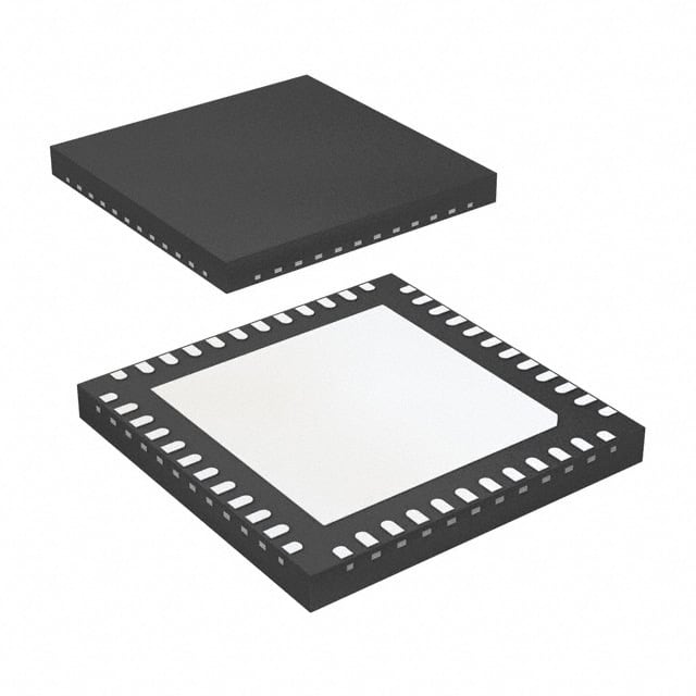
- Part No.:
- PI6CG188Q2ZLQEX
- Manufacturer:
- Diodes Incorporated
- Package:
- 48-VFQFN Exposed Pad
- Datasheet:
-
 PI6CG188Q2ZLQEX.pdf
- Description:
- IC CLOCK GENERATOR 48TQFN
- Quantity:
- Payment:

- Shipping:

Inventory:3,273
Please send an inquiry. Send us your inquiry, and we will respond immediately.
Product details
Overview
PI6CG188Q2ZLQEX from Diodes Incorporated is an 8-output, automotive-grade PCIe Gen4 clock generator with 1.8V supply, 25MHz crystal/CMOS input, and eight differential low-power HCSL outputs featuring on-chip 50Ω termination. It delivers <50ps differential cycle-to-cycle jitter, <60ps output-to-output skew, and AEC-Q100 Grade 2 qualification for use in ADAS domain controllers and automotive infotainment backplanes.
For engineers reviewing the PI6CG188Q2ZLQEX datasheet, PI6CG188Q2ZLQEX pinout, PI6CG188Q2ZLQEX application, or PI6CG188Q2ZLQEX equivalent, key selection criteria include PCIe Gen4 timing compliance, spread-spectrum EMI reduction capability, individual output enable control, SMBus programmability, and integrated HCSL termination eliminating 32 external resistors.
Technical Context
The device implements a proprietary PLL architecture optimized for PCIe Gen1–Gen4 common-clock and separate-reference architectures, with configurable PLL bandwidth (2–5MHz) and CDR reference at 10MHz. It supports three spread-spectrum modulation depths (0%, –0.25%, –0.5%) via tri-level strapping or SMBus, and features dual configuration paths: hardware strapping pins for static setup and 3.3V-tolerant SMBus for dynamic runtime reconfiguration.
All eight HCSL outputs are gated until PLL lock detection, ensuring glitch-free startup. The buffered 1.8V LVCMOS REFOUT provides <1.5ps RMS phase jitter and serves as a low-noise reference for companion SerDes or PHYs, while independent OE# pins per output enable precise power sequencing in multi-rail automotive systems.
Key Specifications
| Parameter | Value and Actual Design Meaning |
|---|---|
| Output Count & Type | 8 × differential HCSL outputs with integrated 50Ω on-die termination per pair |
| Input Reference | 25MHz fundamental-mode crystal or CMOS clock; supports direct XTAL_IN/CLK connection |
| Jitter Performance | Differential cycle-to-cycle jitter <50ps; PCIe Gen4 integrated phase jitter 0.3–0.5ps RMS (10kHz–50MHz) |
| Spread Spectrum | Selectable 0%, –0.25%, or –0.5% triangular modulation at 31.6kHz center frequency |
| Power Supply | 1.8V core (VDD, VDDA, VDD_DIG, VDD_OSC, VDD_REFOUT); 1.05–1.8V output supply (VDDO) |
| Automotive Qualification | AEC-Q100 Grade 2 (–40°C to +105°C ambient), IATF 16949 manufacturing |
| Interface | 3.3V-tolerant SMBus slave interface with 7-bit address; supports block read/write and register-level slew/amplitude control |
Pinout & Package
Package: 48-lead 6mm × 6mm TQFN (exposed pad), RoHS-compliant, halogen- and antimony-free.
| Pin/Terminal | Circuit Role | Design Meaning |
|---|---|---|
| Q0+ / Q0– to Q7+ / Q7– (Pins 15,16,18,19,23,24,26,27,32,33,35,36,41,42,44,45) | Differential HCSL clock outputs | True/complement pairs delivering 100MHz PCIe clocks; each pair includes on-chip 50Ω termination to reduce layout complexity and BOM count |
| OE0# to OE7# (Pins 14,17,25,28,34,37,43,46) | Active-low output enable controls | Individually disable corresponding Qn+ / Qn– pair; internal pulldown ensures default enabled state at power-up |
| XTAL_IN/CLK (Pin 3), XTAL_OUT (Pin 4) | Clock reference interface | Accepts 25MHz crystal (fundamental mode, 8pF load) or CMOS input; internal 5pF capacitance simplifies crystal matching |
| SADR/REFOUT (Pin 7), REFOUT (LVCMOS) | Configurable reference output | Configurable as SMBus address latch (SADR) or 1.8V LVCMOS buffered reference clock with <1.5ps RMS phase jitter |
| SS_SEL_TRI (Pin 1), PD# (Pin 48) | Strap control & power management | Tri-level pin selects spread-spectrum depth at power-up; PD# enters/exits low-power mode with 20–300µs wake latency |
| SCLK / SDATA (Pins 10,11) | SMBus interface | 3.3V-tolerant serial bus supporting dynamic configuration of slew rate, amplitude, and SS settings without reset |
Key Features
| Feature | Design Value |
|---|---|
| On-chip HCSL termination | Eliminates 32 external 50Ω resistors per output pair, reducing PCB area and improving signal integrity in dense automotive layouts |
| Per-output slew rate control | Four programmable settings (1.1–4.0 V/ns) per output via SMBus registers to optimize EMI vs. edge speed trade-offs |
| Individual output enable logic | Eight dedicated OE# pins allow selective activation of clock domains during boot, sleep, or functional safety transitions |
| PLL lock-gated outputs | Differential outputs remain blocked until PLL achieves stable lock, preventing metastability in downstream SerDes receivers |
| Wake-on-LAN current optimization | Sub-1mA total supply current (IDD_WL + IDDO_WL + IDDA_WL) in low-power mode with REFOUT active and all Q outputs disabled |
Applications
| ADAS Domain Controller | Automotive Infotainment Backplane |
|---|---|
Use Scenario: Synchronizing multiple high-speed camera, radar, and sensor fusion processors in a centralized vehicle perception system. IC Role / Device Role / Timing Role: Primary PCIe Gen4 clock source distributing 100MHz reference to multiple SoCs and FPGAs across a multi-layer automotive PCB. Use Value: Sub-50ps cycle-to-cycle jitter ensures deterministic timing margins for PCIe Gen4 x16 links operating at 16 GT/s, meeting ASIL-B timing integrity requirements. | Use Scenario: Clocking display processors, audio DSPs, and telematics modems on a shared infotainment mainboard with strict EMI limits. IC Role / Device Role / Timing Role: Low-jitter, spread-spectrum-capable clock generator enabling simultaneous operation of multiple high-speed peripherals without violating CISPR 25 Class 5 radiated emissions. Use Value: Selectable –0.5% spread spectrum reduces peak EMI by >10dB at 100MHz harmonics, eliminating need for additional ferrite beads or shielding. |
| Vehicle Telematics Gateway | Automotive Ethernet Switch Timing |
Use Scenario: Providing synchronized clocks to LTE/V2X modems, GNSS receivers, and secure MCU subsystems within a telematics control unit. IC Role / Device Role / Timing Role: Dual-role timing IC supplying both PCIe reference clocks and a clean 25MHz LVCMOS REFOUT for GNSS baseband processing. Use Value: REFOUT phase jitter <1.5ps RMS enables high-precision time-of-arrival measurements required for RTK-GNSS positioning accuracy ≤10cm. | Use Scenario: Generating synchronized 125MHz/250MHz clocks for multi-port automotive Ethernet switches (100BASE-T1/1000BASE-T1). IC Role / Device Role / Timing Role: Programmable clock source supporting flexible output frequencies via external divider chains driven from 100MHz HCSL outputs. Use Value: Individual slew rate control per output allows tuning of edge rates to match trace impedance and minimize reflections on long automotive Ethernet backplanes. |
Equivalent & Alternatives
The following parts are listed as comparable options for similar PCIe clock generation applications.
| Alternative Part | Technical Difference | Application Difference | Selection Advice |
|---|---|---|---|
| IDT8T49N242BGI800 | 8-output PCIe Gen4 clock with JESD204B support; requires external termination; higher supply current (IDDO = 65mA typ) | Targeted at radar data converters requiring JESD204B SYSREF; lacks automotive qualification | Choose only if JESD204B synchronization is required and AEC-Q100 is not mandatory |
| Si53320-D-GM | 6-output PCIe Gen3 clock; no spread spectrum; 3.3V-only supply; lower jitter (35ps c2c) but Gen3-limited | Cost-sensitive non-automotive server/storage applications where Gen4 bandwidth is unnecessary | Select when Gen3 performance suffices and 3.3V supply simplifies power design |
Compared with IDT8T49N242BGI800 and Si53320-D-GM, the PI6CG188Q2ZLQEX uniquely combines AEC-Q100 Grade 2 qualification, integrated HCSL termination, and selectable spread spectrum-enabling single-part compliance with automotive EMI, reliability, and layout constraints that alternatives cannot satisfy simultaneously.
Availability
PI6CG188Q2ZLQEX is available at Aetrix Electronics and suitable for ADAS domain controllers, automotive infotainment backplanes, and vehicle telematics gateways requiring stable component supply, long-term automotive lifecycle support, and AEC-Q100-compliant timing solutions.
Supply support for PI6CG188Q2ZLQEX includes scheduled delivery planning, volume procurement assistance, BOM continuity management, traceable sourcing, and lifecycle availability coordination for OEM customers, industrial embedded developers, connected-device designers, and electronics production programs.
Manufacturer
Diodes Incorporated is a global manufacturer of discrete semiconductors and analog ICs, specializing in high-reliability power management, signal integrity, and timing solutions for automotive, industrial, and computing markets.
The PI6CG188Q product line delivers PCIe Gen1–Gen4 clock generators engineered specifically for automotive electronics, emphasizing AEC-Q100 qualification, low-jitter PLL design, and EMI-reduction features required in modern vehicle ECUs.
FAQ
What is the minimum startup time from power-on to stable 100MHz HCSL output?
The PI6CG188Q2ZLQEX achieves full startup-including crystal oscillation stabilization, PLL lock, and output enable-in ≤10ms after VDD reaches 1.7V. This is verified under worst-case conditions (–40°C, 1.7V supply, 25MHz crystal). The tLOCK specification confirms PLL lock occurs within 20ms, and tPDLAT guarantees differential outputs enable within 20–300µs after PD# deassertion.
Can the REFOUT pin be used simultaneously as SMBus address latch and clock output?
No. Pin 7 (SADR/REFOUT) operates in one mode only: when configured as SADR (default at power-up), it latches SMBus address and cannot output REFOUT; when configured as REFOUT via SMBus register Byte 0 Bit 7, it delivers the 1.8V LVCMOS buffered reference clock but loses SMBus address functionality. Mode selection is mutually exclusive and must be set before initialization.
How does the tri-level SS_SEL_TRI pin determine spread-spectrum depth?
SS_SEL_TRI (Pin 1) uses voltage thresholds relative to VDD: logic '0' (≤0.25×VDD) selects 0% spread; logic 'M' (0.4–0.6×VDD) selects –0.25%; logic '1' (≥0.75×VDD) selects –0.5%. These states are latched at first PD# high assertion and override SMBus-controlled spread settings until next power cycle or PD# reset.
What is the maximum allowable load capacitance on the XTAL_IN/CLK input?
The XTAL_IN/CLK input has a specified internal capacitance of 5pF and is designed for fundamental-mode 25MHz crystals with 8pF load capacitance. Total effective load-including PCB trace capacitance-must not exceed 10pF to maintain reliable oscillation margin and meet ±50ppm frequency accuracy over temperature and voltage. External loading beyond this risks startup failure or frequency drift.
PI6CG188Q2ZLQEX Specifications
- Product attributes
- Attribute value
- Manufacturer:
- Diodes Incorporated
- Series:
- -
- Package/Case:
- 48-VFQFN Exposed Pad
- Packaging:
- Tape & Reel (TR)
- Product Status:
- Active
- Programmable:
- Not Verified
- Type:
- Clock Generator
- PLL:
- Yes
- Input:
- CMOS, Crystal
- Output:
- CMOS, HCSL
- Number of Circuits:
- 1
- Ratio - Input:Output:
- 1:8
- Differential - Input:Output:
- No/Yes
- Frequency - Max:
- 100MHz
- Divider/Multiplier:
- No/No
- Voltage - Supply:
- 1.7V ~ 1.9V
- Operating Temperature:
- -40°C ~ 105°C (TA)
- Mounting Type:
- Surface Mount
- Grade:
- Automotive
- Qualification:
- AEC-Q100
- Supplier Device Package:
- 48-TQFN (6x6)
PI6CG188Q2ZLQEX FAQ
1.How can I place an order for PI6CG188Q2ZLQEX through Aetrix?
Please submit a Request for Quotation (RFQ) for PI6CG188Q2ZLQEX on Aetrix. Our sales agent will provide a competitive quotation and guide you through the order confirmation once you accept the terms.
2.Are the price and stock information for PI6CG188Q2ZLQEX reliable?
The price and inventory of PI6CG188Q2ZLQEX are updated periodically and may fluctuate due to market conditions. Stock and pricing data are typically refreshed every 24 hours. Quotation validity for PI6CG188Q2ZLQEX is usually 5 days.
3.What payment methods are accepted for PI6CG188Q2ZLQEX?
We accept Wire Transfer, PayPal, Credit Card, Western Union, MoneyGram, and Escrow for PI6CG188Q2ZLQEX transactions.
Note: Certain payment methods may incur a processing fee.
4.How is shipping managed for PI6CG188Q2ZLQEX?
PI6CG188Q2ZLQEX orders can be shipped via leading logistics carriers, including DHL, UPS, FedEx, TNT, or Registered Mail.
Once your PI6CG188Q2ZLQEX order is processed, you will receive an email with the shipment details and tracking number.
Note: Tracking information may take up to 24 hours to appear. Express delivery typically takes 3–5 business days.
5.How can I obtain technical support or documentation for PI6CG188Q2ZLQEX?
For technical support, including PI6CG188Q2ZLQEX datasheets, pinout diagrams, or application guidance, please contact our engineering support team. They can provide detailed documentation and assistance for your PI6CG188Q2ZLQEX requirements.
6.How does Aetrix verify that PI6CG188Q2ZLQEX is sourced from the original manufacturer or authorized distributors?
All PI6CG188Q2ZLQEX products on Aetrix are procured from qualified distributors and authorized channels. Our dedicated quality assurance team conducts strict verification, including traceability checks and, if necessary, third-party testing. This ensures that PI6CG188Q2ZLQEX meets industry standards.
7.What is the process for return or replacement of PI6CG188Q2ZLQEX?
All PI6CG188Q2ZLQEX units undergo pre-shipment inspection (PSI). If there is an issue with PI6CG188Q2ZLQEX, returns or replacements are accepted under the following conditions:
1.Quantity discrepancies, incorrect items, or visible external defects (such as breakage or corrosion), acknowledged by Aetrix.
2.The issue is reported within 90 days of delivery.
3.The PI6CG188Q2ZLQEX part is unused and in its original packaging.
Return procedure for PI6CG188Q2ZLQEX:
1.Submit a request within 90 days.
2.Obtain a Return Material Authorization (RMA) from Aetrix.
PI6CG188Q2ZLQEX Tags

-
CD74HCT4046AM96
Texas Instruments

-
MC14046BDWR2G
onsemi

-
501MILFT
Renesas Electronics Corporation
-
CD74HC7046AM
Texas Instruments

-
CDCVF2505PWR
Texas Instruments

-
RC19004A100GNL#KB0
Renesas Electronics Corporation

-
SI5351A-B-GTR
Skyworks Solutions Inc.

-
CY2305SXI-1T
Infineon Technologies
-
570BILFT
Renesas Electronics Corporation

-
CDCE913PWR
Texas Instruments
-
CY2305SXI-1HT
Infineon Technologies

-
DS1086LU+T
Analog Devices Inc./Maxim Integrated
Tech Hub

An engineering guide to LED driver operation, constant-current and constant-voltage outputs, linear and switching topologies, dimming, IC selection, calculations, replacement compatibility, and fault c…

Operational amplifier guide covering op amp basics, feedback, ideal vs real op amps, common configurations, buffer circuits, offset, bias current, gain-bandwidth, slew rate, rail-to-rail limits and sel…

Jumper cables guide covering safe connection order, red and black clamp placement, final ground connection, cable gauge, length, clamp quality, copper vs CCA cables, jump starter comparison and battery…

LDO regulator guide covering low dropout voltage, power dissipation, thermal design, PSRR, output noise, capacitor stability, adjustable LDO circuits, LDO vs buck converter and datasheet selection chec…

Conditional Access Module guide covering CAM meaning, CI/CI+ interface, smart card authorization, DVB security workflow, TV and set-top box compatibility, internal electronics, ESD protection, connecto…

Guide to electronic component obsolescence covering EOL risk, PCN/PDN notices, last-time buy planning, replacement options, form-fit-function validation, counterfeit risk and BOM lifecycle management.

18650 battery guide covering lithium-ion cell basics, 3.6V/3.7V voltage, 4.2V charging, mAh and Wh capacity, protected cells, chargers, BMS, series-parallel packs, holders, welding and sourcing checks.…

Hall effect sensor guide covering working principle, linear and digital sensors, Arduino circuits, current sensing, speed detection, automotive applications, A3144 examples, signal filtering and datash…

Product Change Notification guide for electronic components, covering PCN meaning, PCN vs PDN/EOL, common change types, risk levels, form-fit-function review, engineering validation, BOM control, LTB/L…

A practical guide to blend door actuators, covering HVAC function, symptoms, location, AC and heater issues, reset and calibration, replacement cost, electrical diagnosis, compatibility checks, and rep…


