
 My Inquiry
 My Account


Diodes Incorporated PI7C9X2G303ELBZXEX
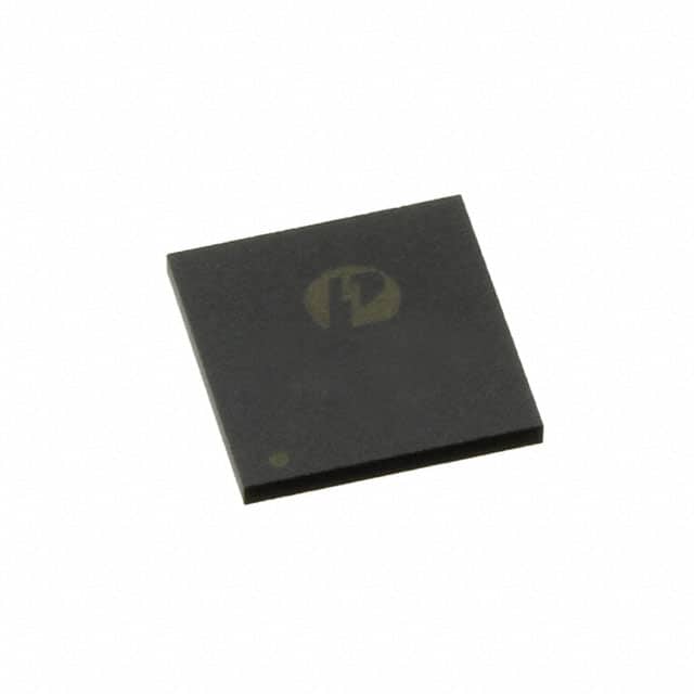
- Part No.:
- PI7C9X2G303ELBZXEX
- Manufacturer:
- Diodes Incorporated
- Category:
- Specialized
- Package:
- 136-VFQFN Dual Rows, Exposed Pad
- Datasheet:
-
 PI7C9X2G303ELBZXEX.pdf
- Description:
- IC INTERFACE SPECIALIZED 136AQFN
- Quantity:
- Payment:

- Shipping:

Inventory:6,915
Please send an inquiry. Send us your inquiry, and we will respond immediately.
Product details
Overview
PI7C9X2G303EL from Diodes Incorporated is a PCI Express Gen 2 packet switch IC with 3 downstream ports, 3-lane total bandwidth, transparent bridging architecture, integrated 100 MHz differential reference clock buffer, and support for 512-byte maximum payload size. It operates at 2.5 GT/s per lane and targets embedded systems requiring PCIe expansion in space-constrained industrial and communications equipment.
For engineers reviewing the PI7C9X2G303EL datasheet, PI7C9X2G303EL pinout, PI7C9X2G303EL application, or PI7C9X2G303EL equivalent, key selection criteria include lane count allocation flexibility, OBFF (Optimized Buffer Flush Forwarding) support, LTR (Latency Tolerance Reporting), EEPROM-based configuration, and JTAG boundary scan capability for system-level debug and validation.
Technical Context
The PI7C9X2G303EL implements a non-transparent, transparent-mode PCIe 2.0 switch with three configurable downstream ports sharing a total of three lanes - enabling 1x+1x+1x or 2x+1x port mapping. Its physical layer supports receiver equalization, programmable transmitter de-emphasis (−3.5 dB, −6 dB), and electrical idle latency control to maintain signal integrity across varying PCB trace lengths.
Internally, it integrates a transaction layer supporting TLP decapsulation/encapsulation, credit-based flow control per VC, TC/VC mapping, and priority-based port arbitration. The device uses an internal configuration space mapped from external EEPROM via SMBus or auto-load mode, eliminating host BIOS dependency for basic initialization.
Key Specifications
| Parameter | Value and Actual Design Meaning |
|---|---|
| PCIe Generation | Gen 2 (2.5 GT/s per lane); enables backward compatibility with Gen 1 while doubling bandwidth over legacy designs. |
| Total Lanes | 3 lanes; allows flexible port configurations such as three 1-lane ports or one 2-lane + one 1-lane port. |
| Port Count | 3 downstream ports; supports daisy-chained or star-topology PCIe endpoint expansion without root complex involvement. |
| Max Payload Size | 512 bytes; reduces transaction overhead and improves throughput for high-bandwidth peripherals like NVMe controllers or FPGAs. |
| Reference Clock | Integrated 100 MHz differential clock buffer with REFCLKO_P/N outputs; eliminates need for external clock generator in compact designs. |
| Power Management | Supports LTR and OBFF; enables low-latency wake-up and optimized power state transitions in battery-sensitive or thermally constrained systems. |
| Configuration Interface | EEPROM (I²C/SMBus) + JTAG; allows field-updatable configuration and boundary-scan testing without host CPU intervention. |
Pinout & Package
This device is housed in a 136-pin QFN package (12 mm × 12 mm, 0.5 mm pitch) with exposed thermal pad, designed for high-density PCB layouts and efficient thermal dissipation in fanless industrial enclosures.
| Pin/Terminal | Circuit Role | Design Meaning |
|---|---|---|
| REFCLKI_P / REFCLKI_N | Differential reference clock input | Accepts 100 MHz differential clock from upstream root complex or oscillator; required for link training and timing synchronization. |
| REFCLKO_P[2:0] / REFCLKO_N[2:0] | Differential reference clock outputs | Provides buffered 100 MHz clocks to up to three downstream endpoints; eliminates need for separate clock distribution ICs. |
| PRSNT[2:1] | Presence detect inputs | Indicates physical presence of downstream cards; used during hot-plug enumeration and link initialization. |
| SMBCLK / SMBDATA | SMBus interface signals | Enable read/write access to internal configuration registers and EEPROM contents for runtime reconfiguration. |
| TCK / TMS / TDI / TDO / TRST_L | JTAG boundary scan interface | Supports IEEE 1149.1-compliant test, debug, and manufacturing verification without dedicated debug headers. |
Key Features
| Feature | Design Value |
|---|---|
| Transparent switching mode | Enables plug-and-play PCIe endpoint expansion without modifying host driver stack or requiring switch-specific software. |
| No-blocking architecture | Guarantees full line-rate throughput across all ports simultaneously, critical for real-time data acquisition and multi-camera vision systems. |
| Programmable de-emphasis | Configurable −3.5 dB or −6 dB transmitter de-emphasis per port; compensates for channel loss without external tuning components. |
| GPIO[7:0] pins | Eight general-purpose I/Os usable for board-level status signaling, reset coordination, or FPGA configuration handshaking. |
| Auto-configuration from EEPROM | Loads port mapping, vendor ID, device ID, and PCIe capabilities on power-up; reduces boot-time dependencies and simplifies firmware integration. |
Applications
| Industrial Machine Vision System | Embedded Network Appliance |
|---|---|
Use Scenario: A compact edge server connects multiple high-resolution cameras and FPGA-based image processors via PCIe expansion. IC Role / Device Role / Timing Role: PCIe packet switch providing isolated, low-latency interconnect between CPU and heterogeneous peripherals. Use Value: Enables deterministic frame capture and processing by eliminating bus contention and supporting 512-byte payloads for efficient DMA transfers. | Use Scenario: A firewall or SD-WAN appliance adds dual 10GbE NICs and hardware crypto acceleration via PCIe add-in modules. IC Role / Device Role / Timing Role: Transparent PCIe bridge managing traffic between SoC host and co-processor cards while maintaining strict timing isolation. Use Value: Maintains wire-speed packet forwarding under load by preventing head-of-line blocking across independent downstream ports. |
| Medical Imaging Controller | Ruggedized Data Acquisition Unit |
Use Scenario: An MRI or CT scanner control unit interfaces with ADC modules, motion controllers, and display subsystems using PCIe expansion. IC Role / Device Role / Timing Role: Reliable PCIe interconnect with OBFF and LTR support for synchronized, low-jitter data streaming and real-time response. Use Value: Reduces system power consumption during idle periods while ensuring sub-microsecond wake latency for time-critical imaging triggers. | Use Scenario: A field-deployable sensor hub aggregates vibration, temperature, and acoustic data from distributed transducers via PCIe-connected DAQ cards. IC Role / Device Role / Timing Role: Robust PCIe switch with JTAG boundary scan and EEPROM-based configuration for maintenance-free operation in harsh environments. Use Value: Simplifies field upgrades and diagnostics through standardized test access and persistent configuration storage unaffected by power cycles. |
Equivalent & Alternatives
The following parts are listed as comparable options for similar PCIe 2.0 packet switch applications.
| Alternative Part | Technical Difference | Application Difference | Selection Advice |
|---|---|---|---|
| PI7C9X2G304EV | Successor part with enhanced 4-port, 4-lane configuration and extended temperature range (−40°C to +105°C). | Required for new designs needing higher port count or extended thermal operation in automotive or outdoor infrastructure. | Select when scalability beyond 3 ports or wider ambient operating range is mandatory; not drop-in compatible due to pinout and register changes. |
| ASM1083 | Intel Gen 1-only (2.5 GT/s) 2-port PCIe switch with no integrated clock buffer or OBFF/LTR support. | Suitable only for cost-sensitive, low-bandwidth applications where Gen 2 features and advanced power management are unnecessary. | Choose only if Gen 1 performance suffices and external clock generation is acceptable; lacks PCIe 2.0 feature set and modern power controls. |
Compared with PI7C9X2G303EL, the PI7C9X2G304EV offers greater port scalability and industrial-grade thermal tolerance but requires layout and firmware updates, while the ASM1083 provides basic Gen 1 switching at lower cost but omits critical Gen 2 features like LTR, OBFF, and integrated clocking - limiting suitability for latency-sensitive or thermally demanding deployments.
Availability
PI7C9X2G303EL is available at Aetrix Electronics and suitable for industrial machine vision systems, embedded network appliances, medical imaging controllers, and ruggedized data acquisition units requiring stable component supply and long-term design continuity.
Supply support for PI7C9X2G303EL includes scheduled delivery planning, volume procurement assistance, BOM continuity management, traceable sourcing, and lifecycle availability coordination for OEM customers, industrial embedded developers, connected-device designers, and electronics production programs.
Manufacturer
Diodes Incorporated is a global manufacturer of discrete semiconductors and integrated circuits, specializing in high-performance analog, logic, and connectivity solutions for industrial, computing, and communications markets.
The PI7C9X2G303EL belongs to Diodes' PCIe packet switch product line, engineered specifically for compact, low-power embedded systems requiring reliable PCIe expansion without host processor overhead or external clocking complexity.
FAQ
Is PI7C9X2G303EL pin-compatible with PI7C9X2G304EV?
No. The PI7C9X2G304EV uses a different 144-pin QFN package and revised pin assignments for additional lanes and GPIOs. Migration requires PCB redesign and firmware updates to accommodate expanded register maps and configuration modes.
Does PI7C9X2G303EL support hot-plug detection?
Yes. It implements PCIe-compliant hot-plug detection via PRSNT[2:1] pins and associated link training logic, enabling dynamic insertion/removal of downstream endpoints without system reset - verified per PCIe Base Specification v2.0 Section 6.6.
Can PI7C9X2G303EL operate without an external EEPROM?
Yes. It supports default configuration mode using internal hardwired settings, though this limits port mapping flexibility and disables vendor-specific identifiers. EEPROM is required for custom configurations, OBFF enablement, and persistent register state retention.
What is the maximum junction temperature for continuous operation?
The datasheet specifies a maximum junction temperature of +125°C under steady-state conditions. Thermal design must ensure θJA ≤ 35°C/W with proper PCB copper pour and thermal via placement beneath the exposed pad to sustain rated performance.
PI7C9X2G303ELBZXEX Specifications
- Product attributes
- Attribute value
- Manufacturer:
- Diodes Incorporated
- Series:
- -
- Package/Case:
- 136-VFQFN Dual Rows, Exposed Pad
- Packaging:
- Tape & Reel (TR)
- Product Status:
- Active
- Applications:
- Wireless
- Interface:
- JTAG
- Voltage - Supply:
- -
- Supplier Device Package:
- 136-aQFN (8x8)
- Grade:
- -
- Qualification:
- -
- Mounting Type:
- Surface Mount
PI7C9X2G303ELBZXEX FAQ
1.How can I place an order for PI7C9X2G303ELBZXEX through Aetrix?
Please submit a Request for Quotation (RFQ) for PI7C9X2G303ELBZXEX on Aetrix. Our sales agent will provide a competitive quotation and guide you through the order confirmation once you accept the terms.
2.Are the price and stock information for PI7C9X2G303ELBZXEX reliable?
The price and inventory of PI7C9X2G303ELBZXEX are updated periodically and may fluctuate due to market conditions. Stock and pricing data are typically refreshed every 24 hours. Quotation validity for PI7C9X2G303ELBZXEX is usually 5 days.
3.What payment methods are accepted for PI7C9X2G303ELBZXEX?
We accept Wire Transfer, PayPal, Credit Card, Western Union, MoneyGram, and Escrow for PI7C9X2G303ELBZXEX transactions.
Note: Certain payment methods may incur a processing fee.
4.How is shipping managed for PI7C9X2G303ELBZXEX?
PI7C9X2G303ELBZXEX orders can be shipped via leading logistics carriers, including DHL, UPS, FedEx, TNT, or Registered Mail.
Once your PI7C9X2G303ELBZXEX order is processed, you will receive an email with the shipment details and tracking number.
Note: Tracking information may take up to 24 hours to appear. Express delivery typically takes 3–5 business days.
5.How can I obtain technical support or documentation for PI7C9X2G303ELBZXEX?
For technical support, including PI7C9X2G303ELBZXEX datasheets, pinout diagrams, or application guidance, please contact our engineering support team. They can provide detailed documentation and assistance for your PI7C9X2G303ELBZXEX requirements.
6.How does Aetrix verify that PI7C9X2G303ELBZXEX is sourced from the original manufacturer or authorized distributors?
All PI7C9X2G303ELBZXEX products on Aetrix are procured from qualified distributors and authorized channels. Our dedicated quality assurance team conducts strict verification, including traceability checks and, if necessary, third-party testing. This ensures that PI7C9X2G303ELBZXEX meets industry standards.
7.What is the process for return or replacement of PI7C9X2G303ELBZXEX?
All PI7C9X2G303ELBZXEX units undergo pre-shipment inspection (PSI). If there is an issue with PI7C9X2G303ELBZXEX, returns or replacements are accepted under the following conditions:
1.Quantity discrepancies, incorrect items, or visible external defects (such as breakage or corrosion), acknowledged by Aetrix.
2.The issue is reported within 90 days of delivery.
3.The PI7C9X2G303ELBZXEX part is unused and in its original packaging.
Return procedure for PI7C9X2G303ELBZXEX:
1.Submit a request within 90 days.
2.Obtain a Return Material Authorization (RMA) from Aetrix.
PI7C9X2G303ELBZXEX Tags

-
NVT4857UKAZ
NXP Semiconductors

-
TCA8418RTWR
Texas Instruments

-
PCA9546APWR
Texas Instruments

-
MD0100N8-G
Microchip Technology

-
PCA9548APW,118
NXP Semiconductors

-
PCA9540BDP,118
NXP Semiconductors

-
PCA9548APWR
Texas Instruments

-
PCA9546APW,118
NXP Semiconductors

-
PTN3360DBS,518
NXP Semiconductors

-
PCA9546ABS,118
NXP Semiconductors

-
PCA9518PWR
Texas Instruments

-
PCA9545APW,118
NXP Semiconductors
Tech Hub

A practical engineering guide to 3.3V and 5V logic compatibility, input thresholds, resistor dividers, translator ICs, MOSFET level shifting, I2C pull-ups, timing limits and power-sequencing risks.

The 74HC595 uses push-pull logic outputs, while the TPIC6B595 uses 50 V open-drain DMOS sinks for higher-power loads. This guide compares timing, current limits, 3.3 V interfacing, load wiring, thermal…

The 74HC595 converts serial data into eight stable parallel outputs. This guide covers pin functions, shift and storage timing, OE and MR behavior, drive-current limits, cascading, voltage compatibilit…

A technical comparison of level-sensitive latches and edge-triggered flip-flops, covering timing windows, setup and hold limits, master–slave operation, time borrowing, race-through, HDL inference and…

A D latch stores one bit while Enable controls when data can pass. This reference covers gate-level operation, truth tables, transparency, setup and hold timing, LE versus OE, common ICs and practical …

An SR latch stores one bit through cross-coupled feedback. This engineering reference covers NOR and NAND implementations, truth tables, forbidden-state recovery, gated operation, switch debouncing, fa…

Latch circuits retain one bit through feedback. This technical reference covers SR and D latches, truth tables, transparency, timing limits, latch-versus-flip-flop behavior, applications and common log…

An engineering guide to LED driver operation, constant-current and constant-voltage outputs, linear and switching topologies, dimming, IC selection, calculations, replacement compatibility, and fault c…

Operational amplifier guide covering op amp basics, feedback, ideal vs real op amps, common configurations, buffer circuits, offset, bias current, gain-bandwidth, slew rate, rail-to-rail limits and sel…

Jumper cables guide covering safe connection order, red and black clamp placement, final ground connection, cable gauge, length, clamp quality, copper vs CCA cables, jump starter comparison and battery…


