
 My Inquiry
 My Account


Diodes Incorporated PI7C9X2G308GPANJE
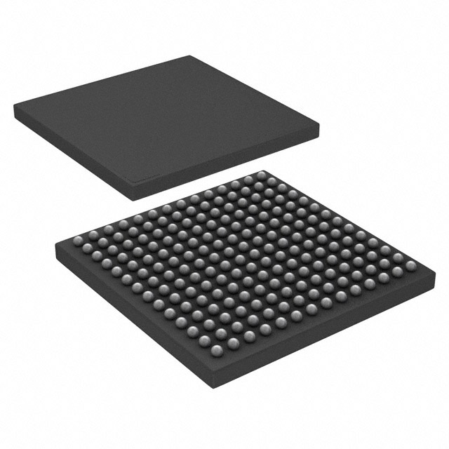
- Part No.:
- PI7C9X2G308GPANJE
- Manufacturer:
- Diodes Incorporated
- Category:
- Specialized
- Package:
- 196-LBGA
- Datasheet:
-
 PI7C9X2G308GPANJE.pdf
- Description:
- IC INTFACE SPECIALIZED 196LBGA
- Quantity:
- Payment:

- Shipping:

Inventory:126
Please send an inquiry. Send us your inquiry, and we will respond immediately.
Product details
Overview
PI7C9X2G308GPANJE from Diodes Incorporated is a 3-port, 8-lane PCI Express Gen 2 packet switch IC designed for PCIe topology expansion in embedded and industrial systems. It supports transparent bridging, hot-plug capability, and configurable port arbitration with 2.5 GT/s per lane, 1.2 V core supply, and integrated 100 MHz differential reference clock buffer.
For engineers reviewing the PI7C9X2G308GPANJE datasheet, PI7C9X2G308GPANJE pinout, PI7C9X2G308GPANJE application, or PI7C9X2G308GPANJE equivalent, key selection criteria include PCIe Gen 2 lane count allocation (x4/x2/x2), EEPROM-based configuration, SMBus/I²C management interface, and LBGA-196 thermal performance under 85°C ambient operation.
Technical Context
The PI7C9X2G308GPANJE implements a full PCIe Gen 2 switch fabric with three downstream ports (Port A: x4, Port B: x2, Port C: x2) and one upstream port, supporting both transparent and non-transparent bridging modes. Its physical layer includes receiver equalization, transmitter de-emphasis control, and electrical idle latency management per lane.
Configuration is handled via on-chip registers mapped to external 2-Kbit I²C/SMBus EEPROM or direct register access. The device integrates a 100 MHz differential REFCLK output buffer and supports spread-spectrum clocking, power management states (L0–L2), and per-port link training with autonomous recovery.
Key Specifications
| Parameter | Value and Actual Design Meaning |
|---|---|
| PCIe Generation | Gen 2 (2.5 GT/s per lane); enables backward-compatible connectivity with legacy PCIe 1.1 endpoints. |
| Lane Configuration | 3-port switch: Upstream x4 + Downstream x4/x2/x2; allows flexible topology partitioning without external retimers. |
| Supply Voltage | Core: 1.2 V ±3%; I/O: 1.5 V/3.3 V selectable; ensures compatibility with mixed-voltage system designs. |
| Reference Clock | Integrated 100 MHz differential REFCLKOP/N buffer; eliminates need for external clock generator in most applications. |
| Management Interface | I²C/SMBus slave interface (400 kHz) + EEPROM auto-load at reset; enables field-updatable configuration without host intervention. |
| Operating Temperature | –40°C to +85°C ambient; qualified for industrial-grade deployment in fanless or convection-cooled enclosures. |
| Package Thermal Resistance | θJA = 27.5°C/W (JEDEC Std); supports sustained 2.5 W typical power dissipation in standard PCB layouts. |
Pinout & Package
The PI7C9X2G308GPANJE is housed in a 196-ball Low-Profile Ball Grid Array (LBGA) package with 0.8 mm pitch, designed for high-density PCB routing and thermal reliability in multi-layer boards.
| Pin/Terminal | Circuit Role | Design Meaning |
|---|---|---|
| REFCLKOP / REFCLKN | Differential reference clock output | Provides 100 MHz LVDS-compatible clock to downstream devices; eliminates external oscillator cost and layout complexity. |
| CLKREQ# / PERST# | PCIe power management and reset control | Enables ASPM L1 entry/exit and cold/warm reset coordination across all ports without host CPU involvement. |
| SCL / SDA | I²C/SMBus serial management interface | Allows runtime register read/write and EEPROM programming via standard system management bus infrastructure. |
| EEPROM_CS# / EEPROM_CLK / EEPROM_DATA | Dedicated SPI-like EEPROM interface | Supports boot-time configuration loading from external 2-Kbit serial EEPROM; independent of I²C bus for fail-safe initialization. |
| VCC_CORE / VCC_IO | Power supply inputs | Separate 1.2 V core and dual-voltage (1.5 V/3.3 V) I/O rails enable mixed-signal interoperability and noise isolation. |
Key Features
| Feature | Design Value |
|---|---|
| Transparent bridging mode | Enables plug-and-play PCIe endpoint expansion without modifying host driver stack or requiring address translation logic. |
| Hot-plug support per port | Allows dynamic insertion/removal of downstream devices (e.g., NVMe SSDs, FPGA accelerators) without system reboot or PCIe enumeration restart. |
| Configurable port arbitration | Weighted round-robin or credit-based arbitration ensures deterministic bandwidth allocation across multiple concurrent traffic streams. |
| Integrated REFCLK buffer | Drives up to four downstream devices directly; reduces BOM count and improves clock skew margin versus discrete clock distribution solutions. |
| EEPROM auto-configuration | Loads port mapping, link speed, and power state settings at power-on; eliminates firmware dependency for basic switch setup. |
Applications
| Industrial Control Gateway | Medical Imaging Subsystem |
|---|---|
Use Scenario: Aggregating multiple PCIe peripherals (motion controllers, vision cameras, I/O modules) into a single x4 upstream link to an ARM-based controller. IC Role / Device Role / Timing Role: PCIe Gen 2 switch providing transparent bridging and per-port hot-plug detection for modular field-replaceable units. Use Value: Reduces host CPU PCIe root port count requirement by 3× while maintaining full Gen 2 bandwidth per downstream device. | Use Scenario: Connecting dual high-speed CT scanner data acquisition cards and a real-time GPU accelerator to a central diagnostic workstation. IC Role / Device Role / Timing Role: Low-latency PCIe switch enabling synchronized DMA transfers between imaging sensors and processing engines. Use Value: Guarantees sub-100 ns inter-port latency and deterministic arbitration for time-critical image reconstruction pipelines. |
| Automotive ADAS Test Bench | Communications Baseband Unit |
Use Scenario: Emulating multi-camera and radar sensor clusters in hardware-in-the-loop (HIL) validation rigs using PCIe-connected FPGA front-ends. IC Role / Device Role / Timing Role: Configurable PCIe switch supporting non-transparent bridging to isolate sensor data domains and enforce memory protection boundaries. Use Value: Enables secure, isolated memory-mapped I/O between safety-critical ADAS subsystems and test host software. | Use Scenario: Interfacing baseband processors, RF transceivers, and packet acceleration ASICs in 5G small-cell radio units with limited PCIe root complex resources. IC Role / Device Role / Timing Role: Lane-aggregating PCIe switch delivering x4 upstream bandwidth while splitting lanes to x2 interfaces for parallel PHY links. Use Value: Doubles effective PCIe endpoint density without adding root complex ports or requiring PCIe switch cascading. |
Equivalent & Alternatives
The following parts are listed as comparable options for similar PCIe Gen 2 switch applications.
| Alternative Part | Technical Difference | Application Difference | Selection Advice |
|---|---|---|---|
| ASM1083 | Single upstream/downstream bridge (not a switch); no multi-port arbitration or EEPROM configuration. | Limited to point-to-point PCIe extension; cannot support >2 endpoints or dynamic port reconfiguration. | Select when only simple PCIe lane replication is needed and system-level topology control resides entirely in host firmware. |
| PI7C9X2G304 | 4-port, 4-lane variant (x1/x1/x1/x1); lower total bandwidth and no x4 upstream capability. | Better suited for distributed low-bandwidth peripherals (e.g., USB 3.0 hubs, SATA controllers) rather than high-throughput imaging or storage. | Choose for cost-sensitive designs where lane count flexibility outweighs aggregate throughput requirements. |
Compared with ASM1083 and PI7C9X2G304, the PI7C9X2G308GPANJE uniquely delivers scalable 8-lane allocation across three ports with autonomous configuration, making it optimal for PCIe expansion in resource-constrained edge computing platforms requiring deterministic bandwidth partitioning.
Availability
PI7C9X2G308GPANJE is available at Aetrix Electronics and suitable for industrial control gateways, medical imaging subsystems, and automotive ADAS test benches requiring stable component supply, long-term lifecycle assurance, and RoHS-compliant green packaging.
Supply support for PI7C9X2G308GPANJE includes scheduled delivery planning, volume procurement assistance, BOM continuity management, traceable sourcing, and lifecycle availability coordination for OEM customers, industrial embedded developers, connected-device designers, and electronics production programs.
Manufacturer
Diodes Incorporated is a global manufacturer of discrete semiconductors and integrated circuits, specializing in high-performance analog, logic, and interconnect solutions for industrial, computing, and communications markets.
The PI7C9X2G308GPANJE belongs to Diodes' PCI Express Switch family, engineered specifically for PCIe Gen 2 topology expansion in space-constrained embedded systems where configurability, thermal efficiency, and management interface flexibility are critical.
FAQ
Does the PI7C9X2G308GPANJE support PCIe Gen 3?
No. The PI7C9X2G308GPANJE is strictly a PCIe Gen 2 device operating at 2.5 GT/s per lane. It does not support 5.0 GT/s signaling, equalization training for Gen 3, or associated protocol extensions such as ASL or ATS. Gen 3 compatibility requires a different switch IC architecture.
Can the PI7C9X2G308GPANJE be configured without external EEPROM?
Yes. Configuration can be performed via I²C/SMBus register writes during runtime or through hard-coded strap pins for basic port enable/disable states. However, full feature set activation-including VC mapping, arbitration weights, and spread-spectrum settings-requires EEPROM or host-initiated register programming.
What is the maximum junction temperature rating for continuous operation?
The PI7C9X2G308GPANJE has a maximum junction temperature (TJ) of +125°C. Under typical 2.5 W power dissipation and standard 4-layer PCB layout with 2 oz copper, this corresponds to reliable operation at +85°C ambient temperature with appropriate thermal vias and copper pour design.
Is there a recommended layout guideline for the REFCLKOP/N traces?
Yes. REFCLKOP/N must be routed as a controlled-impedance differential pair (100 Ω ±10%), length-matched within 5 mils, and kept ≥10 mils from noisy digital signals. Termination resistors (100 Ω differential) are required at the far-end receiver, and no stubs or vias should be placed within the first 10 mm of the switch output pins.
PI7C9X2G308GPANJE Specifications
- Product attributes
- Attribute value
- Manufacturer:
- Diodes Incorporated
- Series:
- GreenPacket™
- Package/Case:
- 196-LBGA
- Packaging:
- Tray
- Product Status:
- Active
- Applications:
- Packet Switch, 3-Port/8-Lane
- Interface:
- PCI Express
- Voltage - Supply:
- -
- Supplier Device Package:
- 196-LBGA (15x15)
- Grade:
- -
- Qualification:
- -
- Mounting Type:
- Surface Mount
PI7C9X2G308GPANJE FAQ
1.How can I place an order for PI7C9X2G308GPANJE through Aetrix?
Please submit a Request for Quotation (RFQ) for PI7C9X2G308GPANJE on Aetrix. Our sales agent will provide a competitive quotation and guide you through the order confirmation once you accept the terms.
2.Are the price and stock information for PI7C9X2G308GPANJE reliable?
The price and inventory of PI7C9X2G308GPANJE are updated periodically and may fluctuate due to market conditions. Stock and pricing data are typically refreshed every 24 hours. Quotation validity for PI7C9X2G308GPANJE is usually 5 days.
3.What payment methods are accepted for PI7C9X2G308GPANJE?
We accept Wire Transfer, PayPal, Credit Card, Western Union, MoneyGram, and Escrow for PI7C9X2G308GPANJE transactions.
Note: Certain payment methods may incur a processing fee.
4.How is shipping managed for PI7C9X2G308GPANJE?
PI7C9X2G308GPANJE orders can be shipped via leading logistics carriers, including DHL, UPS, FedEx, TNT, or Registered Mail.
Once your PI7C9X2G308GPANJE order is processed, you will receive an email with the shipment details and tracking number.
Note: Tracking information may take up to 24 hours to appear. Express delivery typically takes 3–5 business days.
5.How can I obtain technical support or documentation for PI7C9X2G308GPANJE?
For technical support, including PI7C9X2G308GPANJE datasheets, pinout diagrams, or application guidance, please contact our engineering support team. They can provide detailed documentation and assistance for your PI7C9X2G308GPANJE requirements.
6.How does Aetrix verify that PI7C9X2G308GPANJE is sourced from the original manufacturer or authorized distributors?
All PI7C9X2G308GPANJE products on Aetrix are procured from qualified distributors and authorized channels. Our dedicated quality assurance team conducts strict verification, including traceability checks and, if necessary, third-party testing. This ensures that PI7C9X2G308GPANJE meets industry standards.
7.What is the process for return or replacement of PI7C9X2G308GPANJE?
All PI7C9X2G308GPANJE units undergo pre-shipment inspection (PSI). If there is an issue with PI7C9X2G308GPANJE, returns or replacements are accepted under the following conditions:
1.Quantity discrepancies, incorrect items, or visible external defects (such as breakage or corrosion), acknowledged by Aetrix.
2.The issue is reported within 90 days of delivery.
3.The PI7C9X2G308GPANJE part is unused and in its original packaging.
Return procedure for PI7C9X2G308GPANJE:
1.Submit a request within 90 days.
2.Obtain a Return Material Authorization (RMA) from Aetrix.
PI7C9X2G308GPANJE Tags

-
NVT4857UKAZ
NXP USA Inc.

-
TCA8418RTWR
Texas Instruments

-
PCA9546APWR
Texas Instruments

-
MD0100N8-G
Microchip Technology

-
PCA9548APW,118
NXP USA Inc.

-
PCA9540BDP,118
NXP USA Inc.

-
PCA9548APWR
Texas Instruments

-
PCA9546APW,118
NXP USA Inc.

-
PTN3360DBS,518
NXP USA Inc.

-
PCA9546ABS,118
NXP USA Inc.

-
PCA9518PWR
Texas Instruments

-
PCA9545APW,118
NXP USA Inc.
Tech Hub

An engineering guide to LED driver operation, constant-current and constant-voltage outputs, linear and switching topologies, dimming, IC selection, calculations, replacement compatibility, and fault c…

Operational amplifier guide covering op amp basics, feedback, ideal vs real op amps, common configurations, buffer circuits, offset, bias current, gain-bandwidth, slew rate, rail-to-rail limits and sel…

Jumper cables guide covering safe connection order, red and black clamp placement, final ground connection, cable gauge, length, clamp quality, copper vs CCA cables, jump starter comparison and battery…

LDO regulator guide covering low dropout voltage, power dissipation, thermal design, PSRR, output noise, capacitor stability, adjustable LDO circuits, LDO vs buck converter and datasheet selection chec…

Conditional Access Module guide covering CAM meaning, CI/CI+ interface, smart card authorization, DVB security workflow, TV and set-top box compatibility, internal electronics, ESD protection, connecto…

Guide to electronic component obsolescence covering EOL risk, PCN/PDN notices, last-time buy planning, replacement options, form-fit-function validation, counterfeit risk and BOM lifecycle management.

18650 battery guide covering lithium-ion cell basics, 3.6V/3.7V voltage, 4.2V charging, mAh and Wh capacity, protected cells, chargers, BMS, series-parallel packs, holders, welding and sourcing checks.…

Hall effect sensor guide covering working principle, linear and digital sensors, Arduino circuits, current sensing, speed detection, automotive applications, A3144 examples, signal filtering and datash…

Product Change Notification guide for electronic components, covering PCN meaning, PCN vs PDN/EOL, common change types, risk levels, form-fit-function review, engineering validation, BOM control, LTB/L…

A practical guide to blend door actuators, covering HVAC function, symptoms, location, AC and heater issues, reset and calibration, replacement cost, electrical diagnosis, compatibility checks, and rep…


