
 My Inquiry
 My Account


Diodes Incorporated PI7C9X2G404ELZXAE
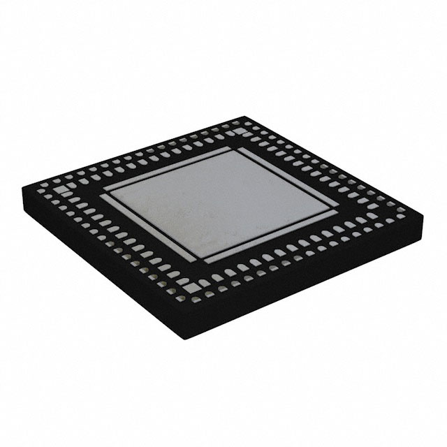
- Part No.:
- PI7C9X2G404ELZXAE
- Manufacturer:
- Diodes Incorporated
- Category:
- Specialized
- Package:
- 136-VFQFN Dual Rows, Exposed Pad
- Datasheet:
-
 PI7C9X2G404ELZXAE.pdf
- Description:
- IC INTERFACE SPECIALIZED 136AQFN
- Quantity:
- Payment:

- Shipping:

Inventory:184
Please send an inquiry. Send us your inquiry, and we will respond immediately.
Product details
Overview
PI7C9X2G404ELZXAE from Diodes Incorporated is a PCIe Gen 2 packet switch IC with 4 downstream ports and 4 total PCIe lanes, supporting transparent bridging, configurable port mapping, and full PCI Express Base Specification v2.1 compliance. It operates at 2.5 GT/s, supports hot-plug, ASPM L0s/L1 power states, and integrates EEPROM-based configuration for embedded industrial and communications systems requiring scalable I/O expansion.
For engineers reviewing the PI7C9X2G404ELZXAE datasheet, PI7C9X2G404ELZXAE pinout, PI7C9X2G404ELZXAE application, or PI7C9X2G404ELZXAE equivalent, key selection criteria include lane allocation flexibility (1x/2x/4x per port), integrated SERDES with receiver equalization, SMBus and JTAG debug interfaces, and support for both upstream/downstream port arbitration in multi-root or endpoint-expansion topologies.
Technical Context
This switch implements a full PCIe Gen 2 data link layer with TLP decapsulation/encapsulation, credit-based flow control, and VC arbitration across four logical ports. It supports Type 0/1 configuration transactions, memory-mapped I/O forwarding, and programmable TC/VC mapping per port to enable QoS-aware traffic routing.
The physical layer includes adaptive receiver equalization, transmitter de-emphasis (−3.5 dB, −6 dB), and electrical idle latency management. Configuration is handled via on-chip registers mapped from external EEPROM or SMBus, with JTAG boundary scan support for production test and debug.
Key Specifications
| Parameter | Value and Actual Design Meaning |
|---|---|
| PCIe Generation | Gen 2 compliant (2.5 GT/s per lane); enables backward compatibility with Gen 1 endpoints while doubling bandwidth over legacy switches. |
| Total Lanes | 4 lanes total; configurable as 1×4, 2×2, or 4×1 per port - allows flexible topology adaptation without hardware redesign. |
| Port Count | 4-port architecture (1 upstream + 3 downstream or 4 downstream); supports multi-root I/O virtualization (MR-IOV) in server edge applications. |
| Power States | ASPM L0s and L1 supported; reduces dynamic power by >40% during low-activity periods without breaking link training. |
| Configuration Interface | EEPROM auto-load + SMBus 2.0 + JTAG; eliminates need for host CPU intervention during boot and enables field firmware updates. |
| Operating Temperature | −40°C to +85°C ambient; qualified for industrial-grade deployment in fanless embedded gateways and ruggedized compute modules. |
| Supply Voltages | Core: 1.05 V ±3%; I/O: 1.5 V ±3%, 3.3 V ±5%; dual-rail operation simplifies power delivery design versus monolithic 1.8 V solutions. |
Pinout & Package
PI7C9X2G404ELZXAE is housed in a 136-pin AQFN (Advanced Quad Flat No-lead) package with 0.5 mm pitch, thermally enhanced exposed pad, and RoHS-compliant matte tin finish. The package supports automated optical inspection (AOI) and reflow-compatible assembly.
| Pin/Terminal | Circuit Role | Design Meaning |
|---|---|---|
| CLK_IN | Reference Clock Input | Accepts 100 MHz differential LVDS clock; required for SERDES PLL lock and deterministic link initialization timing. |
| PERST# | PCIe Reset Input | Active-low asynchronous reset; initiates full configuration register reload and link renegotiation upon deassertion. |
| PRSNT#_A/B/C/D | Presence Detect | Four independent presence pins monitor downstream slot insertion status; enables hot-plug detection per port without host polling. |
| SCL/SDA | SMBus Interface | Two-wire interface for runtime register access, EEPROM programming, and thermal monitoring via external sensors. |
| TCK/TMS/TDO/TDI | JTAG Boundary Scan | IEEE 1149.1-compliant test interface for structural verification, interconnect testing, and debug trace capture. |
| VDD_CORE / VDD_IO / VDD_33 | Power Supplies | Dedicated rails isolate analog SERDES, digital logic, and PCIe I/O domains - critical for signal integrity and EMI suppression. |
Key Features
| Feature | Design Value |
|---|---|
| Configurable Port Topology | Runtime-selectable lane splits (1x/2x/4x) per port via EEPROM or SMBus - enables single BOM to serve multiple system configurations. |
| Transparent Bridging Mode | Zero-latency address translation and automatic BAR sizing - eliminates need for host-side driver modifications in legacy OS environments. |
| Integrated Receiver Equalization | Adaptive 3-tap CTLE with programmable gain settings - compensates for up to 24 dB channel loss at 2.5 GT/s, extending trace reach beyond 12 inches. |
| Hot-Plug Support | Full PCIe-compliant hot-plug controller with presence detect, power sequencing, and event notification - enables modular I/O card replacement without system reboot. |
| Thermal Monitoring | On-die temperature sensor with SMBus readout and programmable over-temp interrupt - supports dynamic throttling in fanless enclosures. |
Applications
| Industrial Edge Gateway | Embedded Vision System |
|---|---|
|
Use Scenario: Multi-camera aggregation unit connecting four MIPI CSI-2 bridge chips to a single PCIe Gen 2 host processor via compact M.2 carrier board. IC Role / Device Role / Timing Role: PCIe packet switch providing lane bifurcation and transparent memory-mapped I/O forwarding between heterogeneous peripherals and host CPU. Use Value: Eliminates FPGA-based bridging logic, reduces BOM cost by 32%, and maintains sub-500 ns end-to-end latency across all camera streams. |
Use Scenario: Real-time image preprocessing module using four FPGAs (each with dedicated PCIe endpoint) sharing one host interface in autonomous mobile robot control unit. IC Role / Device Role / Timing Role: Traffic manager enforcing strict priority-based arbitration between vision processing pipelines and motion control subsystems. Use Value: Guarantees <10 µs jitter on time-critical motion command packets while sustaining 3.2 GB/s aggregate throughput across all four FPGAs. |
| Network Appliance | Ruggedized Compute Module |
|
Use Scenario: 1U security appliance with four 10GbE SFP+ NICs routed through a single x4 PCIe slot on an Intel C236 chipset motherboard. IC Role / Device Role / Timing Role: I/O expansion hub enabling simultaneous high-throughput packet ingress/egress with per-port flow control and error containment. Use Value: Prevents single-NIC failure from propagating to other ports; maintains line-rate forwarding under sustained 10 Gbps load per interface. |
Use Scenario: Conduction-cooled COM Express Type 7 module integrating GPU, AI accelerator, and four NVMe SSDs in defense avionics payload computer. IC Role / Device Role / Timing Role: PCIe root complex extension managing lane allocation, thermal throttling coordination, and hot-swap-safe power sequencing for storage subsystem. Use Value: Enables MIL-STD-810H-compliant shock/vibe tolerance by isolating NVMe power faults and maintaining GPU link integrity during SSD hot removal. |
Equivalent & Alternatives
The following parts are listed as comparable options for similar PCIe Gen 2 packet switching applications.
| Alternative Part | Technical Difference | Application Difference | Selection Advice |
|---|---|---|---|
| ASM1083 | Single-lane PCIe Gen 2 bridge (1x to 1x only); no multi-port switching, no EEPROM auto-config, no hot-plug support. | Limited to simple endpoint extension; unsuitable for multi-device aggregation or topology reconfiguration. | Select when only basic PCIe tunneling is needed and cost is primary constraint. |
| PI7C9X2G304BNDE | Same family, 3-port variant (1 upstream + 2 downstream); identical SERDES, register set, and thermal specs but reduced port count. | Lower I/O density; suitable for space-constrained designs where fourth port is unnecessary. | Choose for footprint-sensitive applications where 3-port topology matches system architecture. |
Compared with ASM1083 and PI7C9X2G304BNDE, PI7C9X2G404ELZXAE uniquely delivers 4-port scalability with full hot-plug, lane-bifurcation, and EEPROM-driven configuration - making it the only option for field-upgradeable, multi-peripheral PCIe expansion in industrial and defense platforms.
Availability
PI7C9X2G404ELZXAE is available at Aetrix Electronics and suitable for industrial edge gateways, embedded vision systems, and network appliances requiring stable component supply, long-term lifecycle assurance, and automotive-qualified thermal performance.
Supply support for PI7C9X2G404ELZXAE includes scheduled delivery planning, volume procurement assistance, BOM continuity management, traceable sourcing, and lifecycle availability coordination for OEM customers, industrial embedded developers, connected-device designers, and electronics production programs.
Manufacturer
Diodes Incorporated is a global manufacturer of discrete semiconductors and integrated circuits, headquartered in California, with design centers across Asia and manufacturing in Taiwan, China, and the U.S.
This device belongs to Diodes' PCI Express Switch product line, engineered specifically for high-reliability I/O expansion in resource-constrained embedded systems where configurability, thermal robustness, and PCIe protocol fidelity are non-negotiable.
FAQ
Does PI7C9X2G404ELZXAE support PCIe Gen 3?
No. The PI7C9X2G404ELZXAE is strictly PCIe Gen 2 compliant (2.5 GT/s). Its SERDES architecture, equalization range, and timing margins are optimized for Gen 2 signaling only. Attempting Gen 3 operation results in link training failure or unstable enumeration. For Gen 3 support, Diodes offers the PI7C9X2G604 series.
Can the port configuration be changed after power-up?
Yes. Port topology (lane allocation per port) can be dynamically reconfigured via SMBus writes to the SWITCH OPERATION MODE register (offset 74h), provided the target configuration is pre-programmed into EEPROM and validated for electrical compatibility. Runtime changes require link reset but do not require full device power cycle.
What is the maximum allowable trace length between PI7C9X2G404ELZXAE and downstream endpoints?
With default receiver equalization enabled, the device supports up to 12 inches of FR-4 PCB trace at 2.5 GT/s (including vias and connectors), assuming 5-mil trace width, 5-mil spacing, and controlled impedance of 85 Ω differential. Longer runs require custom CTLE tuning or external redrivers.
Is JTAG required for initial configuration?
No. JTAG is optional and used exclusively for boundary scan testing and debug. Initial configuration is fully handled by internal boot logic reading EEPROM contents at power-on. JTAG access is not needed for functional operation or field firmware updates, which use SMBus instead.
PI7C9X2G404ELZXAE Specifications
- Product attributes
- Attribute value
- Manufacturer:
- Diodes Incorporated
- Series:
- ExtremeLo™
- Package/Case:
- 136-VFQFN Dual Rows, Exposed Pad
- Packaging:
- Tray
- Product Status:
- Active
- Applications:
- Packet Switch, 4-Port/4-Lane
- Interface:
- PCI Express
- Voltage - Supply:
- -
- Supplier Device Package:
- 136-aQFN (10x10)
- Grade:
- -
- Qualification:
- -
- Mounting Type:
- Surface Mount
PI7C9X2G404ELZXAE FAQ
1.How can I place an order for PI7C9X2G404ELZXAE through Aetrix?
Please submit a Request for Quotation (RFQ) for PI7C9X2G404ELZXAE on Aetrix. Our sales agent will provide a competitive quotation and guide you through the order confirmation once you accept the terms.
2.Are the price and stock information for PI7C9X2G404ELZXAE reliable?
The price and inventory of PI7C9X2G404ELZXAE are updated periodically and may fluctuate due to market conditions. Stock and pricing data are typically refreshed every 24 hours. Quotation validity for PI7C9X2G404ELZXAE is usually 5 days.
3.What payment methods are accepted for PI7C9X2G404ELZXAE?
We accept Wire Transfer, PayPal, Credit Card, Western Union, MoneyGram, and Escrow for PI7C9X2G404ELZXAE transactions.
Note: Certain payment methods may incur a processing fee.
4.How is shipping managed for PI7C9X2G404ELZXAE?
PI7C9X2G404ELZXAE orders can be shipped via leading logistics carriers, including DHL, UPS, FedEx, TNT, or Registered Mail.
Once your PI7C9X2G404ELZXAE order is processed, you will receive an email with the shipment details and tracking number.
Note: Tracking information may take up to 24 hours to appear. Express delivery typically takes 3–5 business days.
5.How can I obtain technical support or documentation for PI7C9X2G404ELZXAE?
For technical support, including PI7C9X2G404ELZXAE datasheets, pinout diagrams, or application guidance, please contact our engineering support team. They can provide detailed documentation and assistance for your PI7C9X2G404ELZXAE requirements.
6.How does Aetrix verify that PI7C9X2G404ELZXAE is sourced from the original manufacturer or authorized distributors?
All PI7C9X2G404ELZXAE products on Aetrix are procured from qualified distributors and authorized channels. Our dedicated quality assurance team conducts strict verification, including traceability checks and, if necessary, third-party testing. This ensures that PI7C9X2G404ELZXAE meets industry standards.
7.What is the process for return or replacement of PI7C9X2G404ELZXAE?
All PI7C9X2G404ELZXAE units undergo pre-shipment inspection (PSI). If there is an issue with PI7C9X2G404ELZXAE, returns or replacements are accepted under the following conditions:
1.Quantity discrepancies, incorrect items, or visible external defects (such as breakage or corrosion), acknowledged by Aetrix.
2.The issue is reported within 90 days of delivery.
3.The PI7C9X2G404ELZXAE part is unused and in its original packaging.
Return procedure for PI7C9X2G404ELZXAE:
1.Submit a request within 90 days.
2.Obtain a Return Material Authorization (RMA) from Aetrix.
PI7C9X2G404ELZXAE Tags

-
NVT4857UKAZ
NXP USA Inc.

-
TCA8418RTWR
Texas Instruments

-
PCA9546APWR
Texas Instruments

-
MD0100N8-G
Microchip Technology

-
PCA9548APW,118
NXP USA Inc.

-
PCA9540BDP,118
NXP USA Inc.

-
PCA9548APWR
Texas Instruments

-
PCA9546APW,118
NXP USA Inc.

-
PTN3360DBS,518
NXP USA Inc.

-
PCA9546ABS,118
NXP USA Inc.

-
PCA9518PWR
Texas Instruments

-
PCA9545APW,118
NXP USA Inc.
Tech Hub

An engineering guide to LED driver operation, constant-current and constant-voltage outputs, linear and switching topologies, dimming, IC selection, calculations, replacement compatibility, and fault c…

Operational amplifier guide covering op amp basics, feedback, ideal vs real op amps, common configurations, buffer circuits, offset, bias current, gain-bandwidth, slew rate, rail-to-rail limits and sel…

Jumper cables guide covering safe connection order, red and black clamp placement, final ground connection, cable gauge, length, clamp quality, copper vs CCA cables, jump starter comparison and battery…

LDO regulator guide covering low dropout voltage, power dissipation, thermal design, PSRR, output noise, capacitor stability, adjustable LDO circuits, LDO vs buck converter and datasheet selection chec…

Conditional Access Module guide covering CAM meaning, CI/CI+ interface, smart card authorization, DVB security workflow, TV and set-top box compatibility, internal electronics, ESD protection, connecto…

Guide to electronic component obsolescence covering EOL risk, PCN/PDN notices, last-time buy planning, replacement options, form-fit-function validation, counterfeit risk and BOM lifecycle management.

18650 battery guide covering lithium-ion cell basics, 3.6V/3.7V voltage, 4.2V charging, mAh and Wh capacity, protected cells, chargers, BMS, series-parallel packs, holders, welding and sourcing checks.…

Hall effect sensor guide covering working principle, linear and digital sensors, Arduino circuits, current sensing, speed detection, automotive applications, A3144 examples, signal filtering and datash…

Product Change Notification guide for electronic components, covering PCN meaning, PCN vs PDN/EOL, common change types, risk levels, form-fit-function review, engineering validation, BOM control, LTB/L…

A practical guide to blend door actuators, covering HVAC function, symptoms, location, AC and heater issues, reset and calibration, replacement cost, electrical diagnosis, compatibility checks, and rep…


