
 My Inquiry
 My Account


NXP Semiconductors PK60FX512VMD12
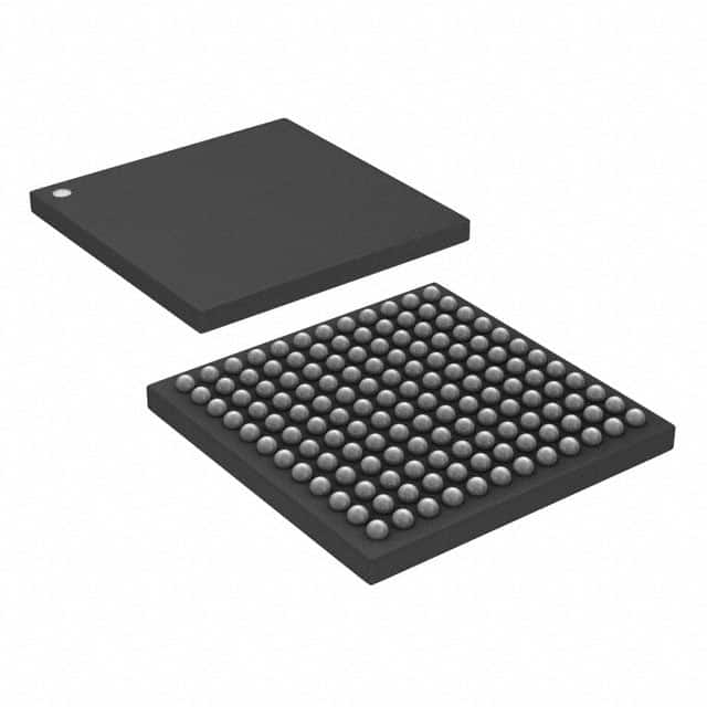
- Part No.:
- PK60FX512VMD12
- Manufacturer:
- NXP Semiconductors
- Category:
- Microcontrollers
- Package:
- 144-LBGA
- Datasheet:
-
 PK60FX512VMD12.pdf
- Description:
- IC MCU 32B 512KB FLASH 144MAPBGA
- Quantity:
- Payment:

- Shipping:

Inventory:2,761
Please send an inquiry. Send us your inquiry, and we will respond immediately.
Product details
Overview
PK60FX512VMD12 from NXP Semiconductors is a Kinetis K60-series ARM Cortex-M4 microcontroller with 512 KB flash, 128 KB SRAM, and 100 MHz CPU frequency. It integrates IEEE 1588 Ethernet MAC, full-speed USB OTG with PHY, dual 16-bit ADCs, two 12-bit DACs, and hardware encryption acceleration. It targets industrial control nodes requiring deterministic timing, secure firmware updates, and real-time network synchronization.
For engineers reviewing the PK60FX512VMD12 datasheet, PK60FX512VMD12 pinout, PK60FX512VMD12 application, or PK60FX512VMD12 equivalent, key selection criteria include IEEE 1588 timestamping accuracy, USB OTG crystal-less operation support, SRAM retention in stop mode, FlexBus interface for external memory expansion, and tamper-detection capability for secure boot validation.
Technical Context
The PK60FX512VMD12 implements an ARM Cortex-M4 core with integrated FPU and 8 KB I/D cache, enabling high-precision sensor fusion and motor control algorithms. Its IEEE 1588 Ethernet MAC includes hardware time stamping logic synchronized to the internal 1588 timer and supports PTP event message capture at sub-microsecond resolution.
It features a configurable FlexBus interface supporting NOR/NAND/SDRAM devices, dual-channel DMA with scatter-gather support, and a low-leakage wake-up unit enabling 5.8 µA stop-mode operation with 4.5 µs wake-up latency. The CAU cryptographic acceleration unit offloads AES-128/256, DES, SHA-1/256, and RNG operations from the CPU.
Key Specifications
| Parameter | Value and Actual Design Meaning |
|---|---|
| CPU Core | ARM Cortex-M4 @ 100 MHz with FPU and 8 KB cache - enables real-time DSP tasks without software floating-point overhead |
| Flash / SRAM | 512 KB program flash + 128 KB SRAM - supports complex protocol stacks (TCP/IP + TLS) and local data buffering |
| Ethernet Interface | IEEE 1588-compliant MAC with hardware timestamping - achieves ±50 ns PTP sync accuracy in industrial PLC backplanes |
| USB Interface | Full-speed USB 2.0 OTG with integrated PHY and crystal-less device mode - eliminates external 12 MHz crystal for cost-sensitive field devices |
| Analog Peripherals | Dual 16-bit SAR ADCs (1 MSPS), dual 12-bit DACs, PGA - supports closed-loop analog I/O in motor drives and sensor transmitters |
| Security Features | CAU crypto accelerator, hardware RNG, tamper detection, flash protection levels - enables secure boot, encrypted OTA updates, and anti-cloning |
| Low-Power Modes | Stop mode: 5.8 µA with SRAM retention and 4.5 µs wake-up - sustains real-time clock and communication state during intermittent operation |
Pinout & Package
PK60FX512VMD12 is housed in a 100-pin LQFP package (14 × 14 mm, 0.5 mm pitch) with exposed thermal pad. Pin functions are defined per the K60 Sub-Family Reference Manual Rev. 6, Table 4-1.
| Pin/Terminal | Circuit Role | Design Meaning |
|---|---|---|
| PTA0–PTA31 | GPIO Port A signals | Configurable digital I/O with interrupt, slew rate, and pull-up/down control - used for status LEDs, relay drivers, and discrete I/O expansion |
| ENET0_RXD0/ENET0_TXD0 | Ethernet MAC data lanes | Dedicated RMII interface pins - connect directly to PHY without level-shifting or external timing compensation |
| USB0_DP/USB0_DM | USB 2.0 full-speed differential pair | Integrated transceiver with on-chip termination - requires only ESD protection diodes and common-mode choke |
| ADC0_SE0–ADC0_SE15 | Analog input channels | 16 single-ended inputs shared with GPIO - supports simultaneous sampling across multiple sensors in building automation controllers |
| VDDA/VSSA | Analog power supply/ground | Independent 3.3 V domain with dedicated filtering - ensures <1 LSB noise in 16-bit ADC conversions |
Key Features
| Feature | Design Value |
|---|---|
| IEEE 1588 Hardware Timestamping | Sub-100 ns capture resolution on PTP sync, delay_req, and delay_resp messages - eliminates software jitter in time-critical motion control networks |
| Crystal-less USB Device Mode | Internal 48 MHz PLL locks to USB SOF packets - removes BOM cost and PCB area of external crystal while maintaining ±0.25% frequency tolerance |
| FlexBus External Memory Interface | 8/16-bit multiplexed address/data bus with programmable wait states - enables direct connection to FPGA-based I/O modules or legacy industrial peripherals |
| Secure Boot with Flash Protection | Four-level flash security (unsecure, secured, backdoor disabled, mass erase disabled) - prevents unauthorized firmware extraction or modification in medical monitoring devices |
| Low-Leakage Wake-Up Unit | 16 independent wake-up sources with configurable edge/polarity - allows selective peripheral activation (e.g., UART RX only) to minimize active current in battery-powered gateways |
Applications
| Industrial PLC I/O Module | Smart Building Gateway |
|---|---|
Use Scenario: Standalone remote I/O node collecting analog sensor data (temperature, pressure) and driving solenoids/relays over Modbus TCP. IC Role / Device Role / Timing Role: Central controller executing real-time control loops, managing Ethernet stack, and synchronizing distributed I/O via IEEE 1588. Use Value: Hardware timestamping ensures deterministic cycle times (<1 ms jitter) across multi-drop EtherNet/IP networks in factory automation. | Use Scenario: Edge gateway aggregating Zigbee/Z-Wave sensor data and forwarding to cloud via TLS-secured Ethernet. IC Role / Device Role / Timing Role: Secure host processor running FreeRTOS, handling USB-based firmware updates, and managing SDHC for local log storage. Use Value: CAU-accelerated AES-256 reduces TLS handshake time by 65% vs. software-only implementation, extending battery life in wireless repeaters. |
| Medical Vital Signs Monitor | Motor Drive Control Board |
Use Scenario: Portable patient monitor acquiring ECG, SpO₂, and respiration waveforms with local display and wired Ethernet upload. IC Role / Device Role / Timing Role: Signal processing hub performing real-time FFT, QRS detection, and waveform rendering using FPU-optimized libraries. Use Value: Dual 16-bit ADCs with PGA enable 120 dB SNR acquisition at 1 kSPS - meets IEC 60601-2-27 clinical accuracy requirements. | Use Scenario: Compact servo drive controlling BLDC motors with position feedback via encoder and Hall sensors. IC Role / Device Role / Timing Role: Motion controller generating PWM outputs, reading quadrature encoders, and communicating over EtherCAT slave interface. Use Value: FlexTimer modules with programmable delay blocks achieve <100 ns PWM dead-time control - prevents shoot-through in 600 V IGBT half-bridges. |
Equivalent & Alternatives
The following parts are listed as comparable options for similar microcontroller applications.
| Alternative Part | Technical Difference | Application Difference | Selection Advice |
|---|---|---|---|
| MKE18F512VLL16 | ARM Cortex-M0+ core, 16 MHz max, no Ethernet MAC or USB OTG PHY - lacks IEEE 1588 and full-speed USB hardware | Suitable for cost-sensitive sensor nodes without network synchronization or host connectivity | Select when deterministic Ethernet timing and USB device functionality are not required |
| MK64FN1M0VLL12 | Same K6x family, 1 MB flash, 256 KB SRAM, 120 MHz CPU - adds SDRAM controller and HS USB OTG (480 Mbps) | Targeted at higher-bandwidth applications like IoT concentrators with video streaming or multi-protocol gateways | Select when larger code footprint, faster USB throughput, or external DRAM expansion is needed |
Compared with PK60FX512VMD12, MKE18F512VLL16 trades networking capability for lower power and cost, while MK64FN1M0VLL12 extends performance and memory for bandwidth-intensive edge processing - both require PCB layout changes due to different pin counts and package footprints.
Availability
PK60FX512VMD12 is available at Aetrix Electronics and suitable for industrial PLC I/O modules, smart building gateways, medical vital signs monitors, and motor drive control boards requiring stable component supply and long-term lifecycle support.
Supply support for PK60FX512VMD12 includes scheduled delivery planning, volume procurement assistance, BOM continuity management, traceable sourcing, and lifecycle availability coordination for OEM customers, industrial embedded developers, connected-device designers, and electronics production programs.
Manufacturer
NXP Semiconductors is a global semiconductor leader focused on secure connectivity solutions for automotive, industrial, and IoT markets, with deep expertise in ARM-based microcontrollers and edge processing.
The Kinetis K60 MCU line was designed specifically for industrial control and building automation systems requiring IEEE 1588 time synchronization, secure firmware updates, and mixed-signal integration in space-constrained LQFP packages.
FAQ
What is the maximum operating frequency of the PK60FX512VMD12?
The PK60FX512VMD12 operates at a maximum CPU frequency of 100 MHz. This speed is achieved using the internal PLL with a 4–24 MHz crystal or external clock source. The ARM Cortex-M4 core includes a floating-point unit and 8 KB of instruction/data cache, enabling efficient execution of control algorithms and signal processing tasks without throttling. The PK60FX512VMD12 maintains this frequency across its full industrial temperature range (–40°C to +105°C).
Does the PK60FX512VMD12 support IEEE 1588 Precision Time Protocol?
Yes, the PK60FX512VMD12 includes a fully integrated IEEE 1588 Ethernet MAC with hardware timestamping logic. It captures precise timestamps on PTP event messages (sync, delay_req, delay_resp) with sub-100 ns resolution. The dedicated 1588 timer and register set allow synchronization accuracy better than ±50 ns in controlled industrial environments - critical for coordinated motion control and distributed I/O systems.
Can the PK60FX512VMD12 operate USB device mode without an external crystal?
Yes, the PK60FX512VMD12 supports crystal-less USB full-speed device mode. Its internal 48 MHz PLL locks directly to the USB Start-of-Frame (SOF) packet stream, eliminating the need for an external 12 MHz crystal. This reduces BOM cost and PCB area while maintaining ±0.25% frequency tolerance - verified per USB-IF compliance testing for PK60FX512VMD12 in device enumeration and data transfer scenarios.
What security features does the PK60FX512VMD12 provide for firmware protection?
The PK60FX512VMD12 provides hardware-enforced flash security with four protection levels: unsecure, secured, backdoor disabled, and mass erase disabled. It also includes a Cryptographic Acceleration Unit (CAU) supporting AES-128/256, SHA-1/256, and RNG operations, plus hardware tamper detection. These features enable secure boot verification and encrypted OTA updates - essential for protecting PK60FX512VMD12-based medical and industrial devices against firmware tampering.
What analog peripherals are integrated into the PK60FX512VMD12?
The PK60FX512VMD12 integrates two 16-bit SAR analog-to-digital converters (ADCs) with up to 1 MSPS aggregate sampling rate, two 12-bit digital-to-analog converters (DACs), a programmable gain amplifier (PGA), and analog comparators. These peripherals share pins with GPIO and support hardware-triggered conversions synchronized to timers or FlexPWM events - enabling high-fidelity sensor acquisition and actuator control in PK60FX512VMD12-based motor drives and environmental monitoring systems.
PK60FX512VMD12 Specifications
- Product attributes
- Attribute value
- Manufacturer:
- NXP Semiconductors
- Package/Case:
- 144-LBGA
- Series:
- Kinetis K60
- Packaging:
- Box
- Product Status:
- Obsolete
- Programmable:
- Not Verified
- Core Processor:
- ARM® Cortex®-M4
- Core Size:
- 32-Bit Single-Core
- Speed:
- 120MHz
- Connectivity:
- CANbus, EBI/EMI, Ethernet, I2C, IrDA, SD, SPI, UART/USART, USB, USB OTG
- Peripherals:
- DMA, I2S, LVD, POR, PWM, WDT
- Number of I/O:
- 100
- Program Memory Size:
- 512KB (512K x 8)
- Program Memory Type:
- FLASH
- EEPROM Size:
- 16K x 8
- RAM Size:
- 128K x 8
- Voltage - Supply (Vcc/Vdd):
- 1.71V ~ 3.6V
- Data Converters:
- A/D 48x16b; D/A 2x12b
- Oscillator Type:
- Internal
- Operating Temperature:
- -40°C ~ 105°C (TA)
- Grade:
- -
- Qualification:
- -
- Mounting Type:
- Surface Mount
- Supplier Device Package:
PK60FX512VMD12 FAQ
1.How can I place an order for PK60FX512VMD12 through Aetrix?
Please submit a Request for Quotation (RFQ) for PK60FX512VMD12 on Aetrix. Our sales agent will provide a competitive quotation and guide you through the order confirmation once you accept the terms.
2.Are the price and stock information for PK60FX512VMD12 reliable?
The price and inventory of PK60FX512VMD12 are updated periodically and may fluctuate due to market conditions. Stock and pricing data are typically refreshed every 24 hours. Quotation validity for PK60FX512VMD12 is usually 5 days.
3.What payment methods are accepted for PK60FX512VMD12?
We accept Wire Transfer, PayPal, Credit Card, Western Union, MoneyGram, and Escrow for PK60FX512VMD12 transactions.
Note: Certain payment methods may incur a processing fee.
4.How is shipping managed for PK60FX512VMD12?
PK60FX512VMD12 orders can be shipped via leading logistics carriers, including DHL, UPS, FedEx, TNT, or Registered Mail.
Once your PK60FX512VMD12 order is processed, you will receive an email with the shipment details and tracking number.
Note: Tracking information may take up to 24 hours to appear. Express delivery typically takes 3–5 business days.
5.How can I obtain technical support or documentation for PK60FX512VMD12?
For technical support, including PK60FX512VMD12 datasheets, pinout diagrams, or application guidance, please contact our engineering support team. They can provide detailed documentation and assistance for your PK60FX512VMD12 requirements.
6.How does Aetrix verify that PK60FX512VMD12 is sourced from the original manufacturer or authorized distributors?
All PK60FX512VMD12 products on Aetrix are procured from qualified distributors and authorized channels. Our dedicated quality assurance team conducts strict verification, including traceability checks and, if necessary, third-party testing. This ensures that PK60FX512VMD12 meets industry standards.
7.What is the process for return or replacement of PK60FX512VMD12?
All PK60FX512VMD12 units undergo pre-shipment inspection (PSI). If there is an issue with PK60FX512VMD12, returns or replacements are accepted under the following conditions:
1.Quantity discrepancies, incorrect items, or visible external defects (such as breakage or corrosion), acknowledged by Aetrix.
2.The issue is reported within 90 days of delivery.
3.The PK60FX512VMD12 part is unused and in its original packaging.
Return procedure for PK60FX512VMD12:
1.Submit a request within 90 days.
2.Obtain a Return Material Authorization (RMA) from Aetrix.
PK60FX512VMD12 Tags

-
ATTINY4-TSHR
Microchip Technology
-
ATTINY10-TSHR
Microchip Technology
-
ATTINY10-TS8R
Microchip Technology

-
ATTINY202-SSNR
Microchip Technology
-
ATTINY202-SSFR
Microchip Technology
-
ATTINY402-SSNR
Microchip Technology

-
PIC16F15213T-I/MF
Microchip Technology
-
PIC16F15213-E/MF
Microchip Technology

-
PIC10F200T-I/OT
Microchip Technology
-
ATTINY412-SSNR
Microchip Technology
-
PIC10F202T-I/OT
Microchip Technology

-
ATTINY404-SSNR
Microchip Technology
Tech Hub

A practical engineering guide to 3.3V and 5V logic compatibility, input thresholds, resistor dividers, translator ICs, MOSFET level shifting, I2C pull-ups, timing limits and power-sequencing risks.

The 74HC595 uses push-pull logic outputs, while the TPIC6B595 uses 50 V open-drain DMOS sinks for higher-power loads. This guide compares timing, current limits, 3.3 V interfacing, load wiring, thermal…

The 74HC595 converts serial data into eight stable parallel outputs. This guide covers pin functions, shift and storage timing, OE and MR behavior, drive-current limits, cascading, voltage compatibilit…

A technical comparison of level-sensitive latches and edge-triggered flip-flops, covering timing windows, setup and hold limits, master–slave operation, time borrowing, race-through, HDL inference and…

A D latch stores one bit while Enable controls when data can pass. This reference covers gate-level operation, truth tables, transparency, setup and hold timing, LE versus OE, common ICs and practical …

An SR latch stores one bit through cross-coupled feedback. This engineering reference covers NOR and NAND implementations, truth tables, forbidden-state recovery, gated operation, switch debouncing, fa…

Latch circuits retain one bit through feedback. This technical reference covers SR and D latches, truth tables, transparency, timing limits, latch-versus-flip-flop behavior, applications and common log…

An engineering guide to LED driver operation, constant-current and constant-voltage outputs, linear and switching topologies, dimming, IC selection, calculations, replacement compatibility, and fault c…

Operational amplifier guide covering op amp basics, feedback, ideal vs real op amps, common configurations, buffer circuits, offset, bias current, gain-bandwidth, slew rate, rail-to-rail limits and sel…

Jumper cables guide covering safe connection order, red and black clamp placement, final ground connection, cable gauge, length, clamp quality, copper vs CCA cables, jump starter comparison and battery…


