
 My Inquiry
 My Account


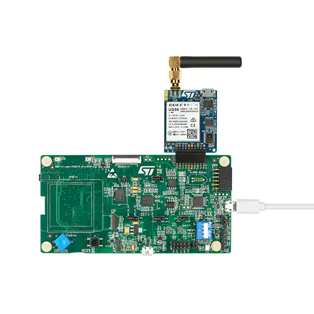
STMicroelectronics P-L496G-CELL01
- Part No.:
- P-L496G-CELL01
- Manufacturer:
- STMicroelectronics
- Category:
- Embedded MCU, DSP Evaluation Boards
- Package:
- Datasheet:
-
 P-L496G-CELL01.pdf
- Description:
- DISCOVERY STM32L496AGI6 EVAL BRD
- Quantity:
- Payment:

- Shipping:

Inventory:1,323
Please send an inquiry. Send us your inquiry, and we will respond immediately.
Product details
Overview
P-L496G-CELL01 from STMicroelectronics is an ultra-low-power Arm® Cortex®-M4 32-bit microcontroller with FPU, 100 DMIPS performance at 80 MHz, 1 MB flash, 320 KB SRAM, USB OTG FS, hardware-accelerated SHA-256 (HASH), and integrated SMPS support. It operates from 1.71–3.6 V across –40 °C to 125 °C and delivers 37 µA/MHz in SMPS-run mode-enabling battery-powered cellular IoT edge nodes with audio, sensing, and secure firmware updates.
For engineers reviewing the P-L496G-CELL01 datasheet, P-L496G-CELL01 pinout, P-L496G-CELL01 application, or P-L496G-CELL01 equivalent, this page provides verified technical context, low-power mode timing, analog peripheral accuracy (12-bit ADC @ 5 Msps), cryptographic accelerator integration, and validated alternative MCU options for cellular-connected embedded designs.
Technical Context
The device integrates an Adaptive Real-time Accelerator (ART) enabling zero-wait-state execution from flash at 80 MHz, and FlexPowerControl architecture supporting seven low-power modes-including 25 nA Shutdown and 426 nA Standby with RTC. Its interconnect matrix routes 20 communication interfaces (2× CAN 2.0B, 2× SAI, 6× USART/LPUART, USB OTG FS) to dual-bank flash and 320 KB SRAM with 64 KB parity-protected region.
Analog subsystem includes three independent 12-bit ADCs (5 Msps, hardware oversampling up to 16-bit), two 12-bit DACs, two op-amps with PGA, two ultra-low-power comparators, and a dedicated Chrom-ART Accelerator (DMA2D) for GUI rendering-each powered from separate supply domains to minimize noise coupling in mixed-signal operation.
Key Specifications
| Parameter | Value and Actual Design Meaning |
|---|---|
| Core | Arm Cortex-M4 with FPU, 80 MHz max frequency, 100 DMIPS, DSP instructions, MPU |
| Memory | 1 MB dual-bank flash (read-while-write), 320 KB SRAM (64 KB with hardware parity) |
| Low-power Run | 37 µA/MHz with external SMPS (VDD12 = 1.10 V), enabling >10-year coin-cell operation in sleep-dominated duty cycles |
| ADC | 3× 12-bit, 5 Msps each; hardware oversampling supports 16-bit effective resolution at reduced sampling rates |
| Crypto | HASH engine supporting SHA-256 for firmware signature verification and secure boot integrity checks |
| Connectivity | USB OTG FS (LPM/BCD), 2× CAN 2.0B, 2× SAI, 4× I²C FM+, 6× USART/UART/LPUART, SDMMC, SWPMI |
| Package | LQFP144 (20 × 20 mm), 144-pin, 0.5 mm pitch, RoHS-compliant, industrial temperature grade (–40 °C to 125 °C) |
Pinout & Package
LQFP144 package with exposed thermal pad; 144-pin square-outline leaded package optimized for industrial PCB assembly and thermal dissipation in compact cellular modem modules.
| Pin/Terminal | Circuit Role | Design Meaning |
|---|---|---|
| VDD, VDDA, VDDIO2 | Main, analog, and I/O power supplies | Independent domains allow analog section isolation and flexible I/O voltage scaling down to 1.08 V |
| PA0–PA15, PB0–PB15, etc. | General-purpose I/Os | Up to 136 fast I/Os; most 5 V-tolerant; 14 pins support independent VDDIO2 supply for mixed-voltage interfacing |
| PC13–PC15 | RTC oscillator inputs | Support 32.768 kHz LSE crystal for calendar-accurate timekeeping in all low-power modes |
| PA11/PA12 | USB OTG FS D+/D– | Dedicated full-speed USB transceiver with internal pull-ups; supports battery charging detection (BCD) |
| PD0/PD1 | OSC_IN/OSC_OUT | 4–48 MHz external crystal interface for system clock generation with ±20 ppm stability |
Key Features
| Feature | Design Value |
|---|---|
| FlexPowerControl architecture | Enables 25 nA shutdown current with 5 wakeup pins-critical for wake-on-RF or sensor-triggered cellular transmission |
| ART Accelerator | Eliminates flash wait states at 80 MHz, reducing active-mode energy per instruction by ~18% vs non-cached execution |
| Dual-bank flash + ROP | Allows secure over-the-air (OTA) firmware updates with rollback protection and readout prevention of sensitive code sections |
| Chrom-ART Accelerator (DMA2D) | Offloads GUI layer composition and image blending from CPU-reducing display update latency in HMI applications |
| Hardware HASH (SHA-256) | Performs cryptographic hashing in <100 µs per 64-byte block-accelerating secure boot and firmware validation |
Applications
| Cellular IoT Sensor Node | Secure Firmware Update Gateway |
|---|---|
Use Scenario: Battery-powered environmental monitor with LTE-M/NB-IoT connectivity, temperature/humidity/pressure sensing, and periodic data upload. IC Role / Device Role / Timing Role: Main application processor managing sensor acquisition, crypto-signed payload generation, cellular modem control, and ultra-low-power sleep scheduling. Use Value: 25 nA shutdown current extends 2000 mAh Li-SOCl₂ battery life beyond 12 years; SHA-256 acceleration ensures OTA update integrity without CPU overhead. | Use Scenario: Industrial gateway aggregating Modbus RTU data from field devices and relaying via LTE to cloud platform with signed firmware distribution. IC Role / Device Role / Timing Role: Secure bootloader and update orchestrator verifying SHA-256 signatures before flashing new firmware to dual-bank flash. Use Value: Dual-bank flash enables atomic firmware swaps with rollback; hardware HASH reduces signature verification time from 120 ms to <8 ms per 4 KB block. |
| Audio-Enabled Wearable | Smart Meter with Tamper Detection |
Use Scenario: Voice-controlled health band with MEMS microphone input, voice activity detection, and Bluetooth LE audio streaming. IC Role / Device Role / Timing Role: Audio preprocessing unit using 2× SAI interfaces for I²S mic input and codec output, plus DMA2D for OLED menu rendering. Use Value: 2× SAI with FIFO buffering enables glitch-free 48 kHz stereo capture; low-power run mode (37 µA/MHz) sustains 7-day battery life with 5% audio duty cycle. | Use Scenario: Electricity meter with optical pulse counting, magnetic tamper sensing, and secure remote firmware updates over PLC or NB-IoT. IC Role / Device Role / Timing Role: System controller handling metrology ADC sampling, tamper interrupt response (<5 µs wakeup from Stop mode), and encrypted firmware validation. Use Value: 5 µs wakeup from Stop mode ensures immediate response to magnetic tamper events; 12-bit ADC oversampling achieves 16-bit effective resolution for precision energy measurement. |
Equivalent & Alternatives
The following parts are listed as comparable options for similar ultra-low-power Arm Cortex-M4 MCU applications.
| Alternative Part | Technical Difference | Application Difference | Selection Advice |
|---|---|---|---|
| STM32L4R9AII6 | 2 MB flash, 640 KB SRAM, LCD-TFT controller, no SMPS support, higher active current (42 µA/MHz) | Better suited for high-resolution color displays; lacks integrated SMPS for ultra-low quiescent systems | Select when GUI complexity demands TFT controller and larger memory, and external DC-DC is acceptable |
| STM32U575ZIT6 | Arm Cortex-M33, TrustZone, 2 MB flash, 1 MB SRAM, 18 nA shutdown, no USB OTG FS, no SAI | Superior security and lower shutdown current; missing audio interfaces and full-speed USB required for cellular modem host control | Select for highest-security applications where audio/USB are handled externally or omitted |
Compared with STM32L4R9AII6 and STM32U575ZIT6, P-L496G-CELL01 uniquely balances cellular modem host capability (USB OTG FS + 2× SAI), ultra-low SMPS-run current (37 µA/MHz), and SHA-256 acceleration-making it optimal for cost-constrained, battery-operated cellular edge nodes requiring integrated audio and secure firmware agility.
Availability
P-L496G-CELL01 is available at Aetrix Electronics and suitable for cellular IoT sensor nodes, secure firmware update gateways, audio-enabled wearables, and smart meters requiring stable component supply across extended product lifecycles.
Supply support for P-L496G-CELL01 includes scheduled delivery planning, volume procurement assistance, BOM continuity management, traceable sourcing, and lifecycle availability coordination for OEM customers, industrial embedded developers, connected-device designers, and electronics production programs.
Manufacturer
STMicroelectronics is a global semiconductor leader headquartered in Geneva, Switzerland, designing and manufacturing microcontrollers, power management ICs, sensors, and automotive semiconductors since 1987.
The STM32L4 series targets ultra-low-power embedded applications demanding long battery life, rich analog integration, and secure firmware execution-specifically optimized for IoT endpoints, portable medical devices, and smart utility infrastructure.
FAQ
What is the minimum supply voltage for P-L496G-CELL01 in Run mode with SMPS enabled?
The minimum supply voltage is 1.71 V across the full industrial temperature range (–40 °C to 125 °C). When using the external SMPS configuration, VDD12 must be regulated to 1.10 V ±3%, while main VDD remains within 1.71–3.6 V. This dual-rail setup enables the 37 µA/MHz efficiency figure cited in the datasheet under typical conditions.
Does P-L496G-CELL01 support hardware-based public-key cryptography?
No-P-L496G-CELL01 integrates only a SHA-256 hash accelerator (HASH peripheral) and true random number generator (RNG). It does not include dedicated asymmetric crypto engines (e.g., RSA, ECC, or AES accelerators). Public-key operations must be implemented in software using the RNG and HASH blocks for key derivation and signature verification workflows.
Can the LQFP144 package accommodate all 136 GPIOs listed in the datasheet?
No-the LQFP144 package exposes 114 user-accessible I/O pins. The full complement of 136 fast I/Os is only available on the UFBGA169 and WLCSP115 packages. LQFP144 pin count constraints require multiplexing certain functions (e.g., FSMC vs QUADSPI) and omitting some low-power timer or comparator inputs present on larger packages.
Is the 5 µs wakeup time from Stop mode guaranteed across all temperature and voltage conditions?
Yes-the 5 µs wakeup time is specified in the datasheet (Section 6.3.6) as a maximum value under worst-case conditions: VDD = 1.71 V, T = 125 °C, with ART Accelerator disabled and no flash prefetch. At nominal 3.3 V and 25 °C, typical wakeup is ≤2.1 µs. This timing includes clock stabilization and NVIC vector fetch, ensuring deterministic real-time response for RF or sensor interrupts.
P-L496G-CELL01 Specifications
- Product attributes
- Attribute value
- Manufacturer:
- STMicroelectronics
- Series:
- STM32L4
- Packaging:
- Bulk
- Product Status:
- Obsolete
- Type:
- MCU 32-Bit
- Core Processor:
- ARM® Cortex®-M4
- Platform:
- Discovery
- Utilized IC / Part:
- STM32L496
- Mounting Type:
- Fixed
- Contents:
- Board(s)
P-L496G-CELL01 FAQ
1.How can I place an order for P-L496G-CELL01 through Aetrix?
Please submit a Request for Quotation (RFQ) for P-L496G-CELL01 on Aetrix. Our sales agent will provide a competitive quotation and guide you through the order confirmation once you accept the terms.
2.Are the price and stock information for P-L496G-CELL01 reliable?
The price and inventory of P-L496G-CELL01 are updated periodically and may fluctuate due to market conditions. Stock and pricing data are typically refreshed every 24 hours. Quotation validity for P-L496G-CELL01 is usually 5 days.
3.What payment methods are accepted for P-L496G-CELL01?
We accept Wire Transfer, PayPal, Credit Card, Western Union, MoneyGram, and Escrow for P-L496G-CELL01 transactions.
Note: Certain payment methods may incur a processing fee.
4.How is shipping managed for P-L496G-CELL01?
P-L496G-CELL01 orders can be shipped via leading logistics carriers, including DHL, UPS, FedEx, TNT, or Registered Mail.
Once your P-L496G-CELL01 order is processed, you will receive an email with the shipment details and tracking number.
Note: Tracking information may take up to 24 hours to appear. Express delivery typically takes 3–5 business days.
5.How can I obtain technical support or documentation for P-L496G-CELL01?
For technical support, including P-L496G-CELL01 datasheets, pinout diagrams, or application guidance, please contact our engineering support team. They can provide detailed documentation and assistance for your P-L496G-CELL01 requirements.
6.How does Aetrix verify that P-L496G-CELL01 is sourced from the original manufacturer or authorized distributors?
All P-L496G-CELL01 products on Aetrix are procured from qualified distributors and authorized channels. Our dedicated quality assurance team conducts strict verification, including traceability checks and, if necessary, third-party testing. This ensures that P-L496G-CELL01 meets industry standards.
7.What is the process for return or replacement of P-L496G-CELL01?
All P-L496G-CELL01 units undergo pre-shipment inspection (PSI). If there is an issue with P-L496G-CELL01, returns or replacements are accepted under the following conditions:
1.Quantity discrepancies, incorrect items, or visible external defects (such as breakage or corrosion), acknowledged by Aetrix.
2.The issue is reported within 90 days of delivery.
3.The P-L496G-CELL01 part is unused and in its original packaging.
Return procedure for P-L496G-CELL01:
1.Submit a request within 90 days.
2.Obtain a Return Material Authorization (RMA) from Aetrix.
P-L496G-CELL01 Tags
-
SC0915
Raspberry Pi
-
102010428
Seeed Technology Co., Ltd
-
SC0917
Raspberry Pi

-
SC1631
Raspberry Pi
-
102010328
Seeed Technology Co., Ltd
-
102010388
Seeed Technology Co., Ltd
-
4600
Adafruit Industries LLC
-
102010268
Seeed Technology Co., Ltd
-
C124
M5Stack Technology Co., Ltd.
-
3500
Adafruit Industries LLC
-
5302
Adafruit Industries LLC
-
DFR0282
DFRobot
Tech Hub

A practical engineering and sourcing framework covering lifecycle verification, lifetime-buy calculations, replacement qualification, supplier checks and counterfeit-risk controls.

TTL and CMOS logic families differ in thresholds, loading, output drive, power and timing. This engineering guide compares 74HC and 74HCT, calculates noise margins and checks 3.3 V/5 V compatibility.

A practical engineering guide to 3.3V and 5V logic compatibility, input thresholds, resistor dividers, translator ICs, MOSFET level shifting, I2C pull-ups, timing limits and power-sequencing risks.

The 74HC595 uses push-pull logic outputs, while the TPIC6B595 uses 50 V open-drain DMOS sinks for higher-power loads. This guide compares timing, current limits, 3.3 V interfacing, load wiring, thermal…

The 74HC595 converts serial data into eight stable parallel outputs. This guide covers pin functions, shift and storage timing, OE and MR behavior, drive-current limits, cascading, voltage compatibilit…

A technical comparison of level-sensitive latches and edge-triggered flip-flops, covering timing windows, setup and hold limits, master–slave operation, time borrowing, race-through, HDL inference and…

A D latch stores one bit while Enable controls when data can pass. This reference covers gate-level operation, truth tables, transparency, setup and hold timing, LE versus OE, common ICs and practical …

An SR latch stores one bit through cross-coupled feedback. This engineering reference covers NOR and NAND implementations, truth tables, forbidden-state recovery, gated operation, switch debouncing, fa…

Latch circuits retain one bit through feedback. This technical reference covers SR and D latches, truth tables, transparency, timing limits, latch-versus-flip-flop behavior, applications and common log…

An engineering guide to LED driver operation, constant-current and constant-voltage outputs, linear and switching topologies, dimming, IC selection, calculations, replacement compatibility, and fault c…


