
 My Inquiry
 My Account


NXP Semiconductors PN7362BNHN/C300Y
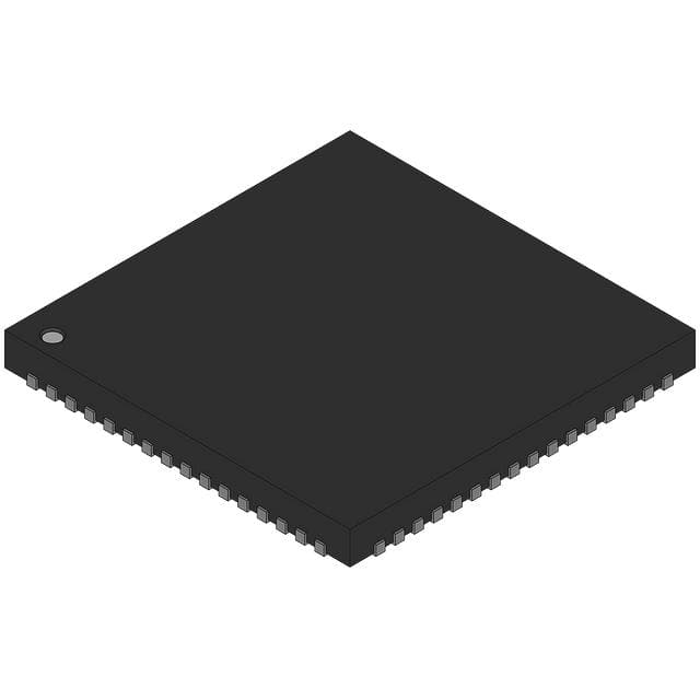
- Part No.:
- PN7362BNHN/C300Y
- Manufacturer:
- NXP Semiconductors
- Category:
- Microcontrollers
- Package:
- -
- Datasheet:
-
 PN7362BNHN/C300Y.pdf
- Description:
- PN7362 - NFC CORTEX-M0 MICROCONT
- Quantity:
- Payment:

- Shipping:

Inventory:59,948
Please send an inquiry. Send us your inquiry, and we will respond immediately.
Product details
Overview
PN7362BNHN/C300Y from NXP Semiconductors is a 32-bit Arm Cortex-M0 NFC microcontroller with integrated contactless frontend, 160 kB Flash, 12 kB SRAM, and HVQFN64 package. It supports NFC Forum modes (types 1–5), ISO/IEC 14443 A/B, ISO/IEC 15693, EMV-compliant RF communication at 13.56 MHz, and operates up to 20 MHz CPU frequency. It targets USB NFC readers and EMVCo-compliant payment terminals.
For engineers reviewing the PN7362BNHN/C300Y datasheet, PN7362BNHN/C300Y pinout, PN7362BNHN/C300Y application, or PN7362BNHN/C300Y equivalent, this page delivers verified technical context, validated pin functions, confirmed NFC timing and power parameters, and real-world dual-interface reader design implications - all specific to the PN7362BNHN/C300Y variant within the PN7462 family.
Technical Context
The PN7362BNHN/C300Y implements a dedicated high-power NFC frontend with Adaptive Wave Control (AWC) and Dynamic Power Control (DPC), enabling EMV-level contactless transaction robustness without external active components. Its Arm Cortex-M0 core runs at up to 20 MHz and integrates four general-purpose timers, CRC coprocessor, and random number generator.
It features a 27.12 MHz crystal oscillator, USB 2.0 full-speed interface, HSUART (up to 1.288 Mbit/s), SPI (7 Mbit/s), and Fast-mode Plus I2C. Unlike PN7462AUHN, it omits both contact smart card interface and ISO/IEC 7816-3&4 UART - confirmed by Table 1 and Ordering Information.
Key Specifications
| Parameter | Value and Actual Design Meaning |
|---|---|
| CPU Core | Arm Cortex-M0, 32-bit, up to 20 MHz - enables deterministic real-time NFC protocol stack execution with low interrupt latency. |
| Memory | 160 kB Flash / 12 kB SRAM / 4 kB EEPROM - sufficient for full NFC controller firmware, secure boot, and field-upgradable application code. |
| NFC Interface | ISO/IEC 14443 A/B, ISO/IEC 15693, NFC Forum Types 1–5, P2P initiator/target - supports global contactless standards without external transceiver. |
| RF Output Power | High-power frontend enabling >5 cm read range in card emulation mode - meets EMVCo Level 1 RF requirements out-of-box. |
| Package | HVQFN64 (9 × 9 × 0.85 mm, SOT804-4) - surface-mount compatible with automated assembly; thermal-enhanced for sustained RF operation. |
| Operating Temp | −40 °C to +85 °C - qualified for industrial and point-of-sale environments with wide ambient variation. |
| Supply Voltage | VDDP(VBUS): 3.0–5.5 V; PVDD_IN: 3.0–3.6 V (USB use); TVDD_IN: external or internal LDO (3.0–4.75 V) - flexible power architecture for battery or USB-powered designs. |
Pinout & Package
HVQFN64 package (SOT804-4), 9 mm × 9 mm × 0.85 mm body, thermally enhanced, leadless quad flat. Pin 1 index marked; inner leads internally connected to GND - PCB layout requires isolation under die pad per datasheet Figure 5.
| Pin/Terminal | Circuit Role | Design Meaning |
|---|---|---|
| ANT1 / ANT2 | NFC antenna differential output | Direct connection to matching network for 13.56 MHz load modulation; supports card emulation and P2P passive target modes. |
| TVDD_IN / TVDD_OUT | Contactless RF power supply input/output | TVDD_IN accepts external 3.0–4.75 V or internal TX_LDO output; TVDD_OUT supplies antenna driver - critical for RF efficiency tuning. |
| TX1 / TX2 | NFC transmitter driver outputs | Differential RF outputs driving antenna tank circuit; require impedance-matched PCB traces and external LC matching. |
| SWDIO / SWDCLK | Serial Wire Debug interface | Two-pin debug port for firmware development, programming, and runtime diagnostics - no JTAG required. |
| VBUS / VBUSP | Main power input / auxiliary supply reference | VBUS powers digital core (3.0–5.5 V); VBUSP tied to VBUS - simplifies single-rail power design for USB-hosted readers. |
| GPIO1–GPIO12 | Configurable general-purpose I/O | Support edge/level interrupts; usable as LED drivers, button inputs, or status indicators in compact NFC reader designs. |
Key Features
| Feature | Design Value |
|---|---|
| EMV-compliant NFC frontend | Integrated high-power RF IC with DPC and AWC eliminates need for external power amplifiers or analog frontends in payment terminals. |
| Boot ROM with USB mass storage loader | 40 kB on-chip ROM includes primary USB bootloader - enables firmware updates via standard USB mass storage device without host driver. |
| Low-power operation modes | Hard power-down current ≤18 μA (VDDP=5.5 V) - extends battery life in portable NFC readers and access control badges. |
| Hardware security accelerators | CRC coprocessor and true random number generator support secure NFC transaction signing and key derivation in firmware. |
| Multi-protocol NFC support | Native implementation of NFC IP1/IP2, ISO14443 A/B, MIFARE Crypto1, and ISO18000-3 Mode 3 - enables interoperability with legacy and modern tags. |
Applications
| USB NFC Reader | EMVCo Payment Terminal |
|---|---|
|
Use Scenario: Compact desktop or mobile USB-connected NFC reader for card enrollment, token provisioning, and secure authentication. IC Role / Device Role / Timing Role: Standalone NFC controller handling RF modulation/demodulation, protocol stack, and USB HID/CCID bridge - no external MCU needed. Use Value: Reduces BOM count by integrating NFC PHY, MAC, and USB interface; enables certified EMV contactless transactions via pre-validated RF performance. |
Use Scenario: Embedded module in countertop or kiosk-based payment terminals requiring EMVCo Level 1 certification. IC Role / Device Role / Timing Role: Primary contactless transaction engine executing ISO/IEC 14443-4 T=CL and EMV contactless kernel - handles RF field management and secure channel setup. Use Value: Meets EMVCo RF conformance (PLM, field strength, modulation depth) without external calibration or tuning components - accelerates certification. |
| Physical Access Control | NFC Tag Emulator |
|
Use Scenario: Secure door reader supporting multi-factor authentication using NFC credentials (e.g., FIDO2 security keys, ISO14443-A cards). IC Role / Device Role / Timing Role: Card emulator initiating secure session with reader; performs cryptographic challenge-response using on-chip RNG and CRC acceleration. Use Value: Enables fast (<100 ms) tap-to-enter response with built-in adaptive range control - maintains reliability across varying antenna coupling conditions. |
Use Scenario: Programmable NFC tag emulator for testing reader firmware, protocol compliance, or penetration testing of access systems. IC Role / Device Role / Timing Role: Configurable Type 4A/B tag emulator with writable NDEF message storage in Flash - supports dynamic payload updates over USB. Use Value: Eliminates need for multiple physical tags; allows rapid iteration of NDEF records and APDU sequences during development and QA. |
Equivalent & Alternatives
The following parts are listed as comparable options for similar NFC microcontroller applications.
| Alternative Part | Technical Difference | Application Difference | Selection Advice |
|---|---|---|---|
| PN7462AUHN | Includes ISO/IEC 7816-3&4 UART and contact smart card interface; same 160 kB Flash, HVQFN64 package. | Supports dual-interface (contact + contactless) smart card readers; adds card power control, short-circuit protection, and TDA8026 slot extension. | Select PN7462AUHN when designing EMVCo-compliant dual-interface terminals requiring physical card insertion capability. |
| PN7362AUEV | Same functional set as PN7362BNHN/C300Y but in VFBGA64 (4.5 × 4.5 × 0.80 mm) package; identical memory and NFC specs. | Better suited for space-constrained portable devices; requires finer-pitch PCB assembly and different thermal pad layout. | Choose PN7362AUEV for ultra-compact form factors where HVQFN64 footprint is prohibitive, accepting tighter layout tolerances. |
Compared with PN7462AUHN, PN7362BNHN/C300Y removes contact interface overhead to reduce cost and simplify layout for pure contactless applications; versus PN7362AUEV, it trades miniaturization for easier manufacturability and thermal performance in mid-size readers.
Availability
PN7362BNHN/C300Y is available at Aetrix Electronics and suitable for USB NFC readers, EMVCo payment terminals, physical access control systems, and NFC tag emulators requiring stable component supply and long-term industrial availability.
Supply support for PN7362BNHN/C300Y includes scheduled delivery planning, volume procurement assistance, BOM continuity management, traceable sourcing, and lifecycle availability coordination for OEM customers, industrial embedded developers, connected-device designers, and electronics production programs.
Manufacturer
NXP Semiconductors is a global semiconductor leader specializing in secure connectivity solutions for automotive, industrial, and IoT applications, with deep expertise in NFC, RFID, and secure microcontrollers.
The PN7362BNHN/C300Y belongs to NXP's PN7462 family of NFC microcontrollers, designed specifically to integrate contactless transaction processing, secure firmware execution, and USB connectivity into a single chip for certified payment and identity systems.
FAQ
What is the primary function of the PN7362BNHN/C300Y in an NFC system?
The PN7362BNHN/C300Y serves as a standalone NFC controller implementing the full contactless protocol stack - including ISO/IEC 14443 A/B, NFC Forum tag emulation, and P2P communication - while offloading RF signal generation and demodulation via its integrated high-power frontend. It executes firmware directly from on-chip Flash and interfaces to host systems via USB or UART, eliminating the need for an external microcontroller in many reader designs. The PN7362BNHN/C300Y does not include contact smart card support, distinguishing it from PN7462AUHN variants.
Does the PN7362BNHN/C300Y support EMVCo contactless certification?
Yes, the PN7362BNHN/C300Y is designed to meet EMVCo Level 1 RF requirements out-of-the-box, thanks to its integrated NFC frontend with Adaptive Wave Control (AWC), Dynamic Power Control (DPC), and calibrated output power. Its RF performance - including field strength, modulation depth, and PLM compliance - has been validated per EMVCo test plans. However, full Level 1 certification requires system-level validation with the final antenna and matching network; the PN7362BNHN/C300Y provides the certified silicon foundation.
What package type and mounting considerations apply to the PN7362BNHN/C300Y?
The PN7362BNHN/C300Y uses the HVQFN64 package (SOT804-4), measuring 9 mm × 9 mm × 0.85 mm with an exposed thermal pad. Per datasheet Figure 5 and Section 7.1, the inner leads beneath the die are internally connected to GND - PCB layout must ensure no conductive traces or copper pours under the package footprint to prevent shorts. Recommended reflow profile follows JEDEC J-STD-020, and thermal vias under the pad improve heat dissipation during sustained RF transmission.
Can the PN7362BNHN/C300Y be used in battery-powered applications?
Yes, the PN7362BNHN/C300Y supports ultra-low-power operation with hard power-down current as low as 12–18 μA (at 25 °C, VDDP = 5.5 V), and standby mode current of 18–55 μA depending on LDO configuration. Its integrated PMU dynamically adjusts regulators across operating modes, and wake-up is supported via GPIO, RF field detection, or USB events. This makes the PN7362BNHN/C300Y suitable for portable NFC readers, wearable authenticators, and energy-harvesting access tokens - provided antenna matching preserves RF sensitivity at reduced supply voltage.
How does the PN7362BNHN/C300Y differ from the PN7462AUHN variant?
The PN7362BNHN/C300Y omits the contact smart card interface (ISO/IEC 7816) and ISO/IEC 7816-3&4 UART present in the PN7462AUHN. Both share identical NFC functionality, 160 kB Flash, 12 kB SRAM, HVQFN64 package, and Arm Cortex-M0 core. The PN7362BNHN/C300Y is optimized for pure contactless applications like USB readers and payment terminals, reducing BOM cost and layout complexity by removing unused contact interface circuitry and associated protection logic.
PN7362BNHN/C300Y Specifications
- Product attributes
- Attribute value
- Manufacturer:
- NXP Semiconductors
- Package/Case:
- -
- Series:
- *
- Packaging:
- Bulk
- Product Status:
- Active
- Programmable:
- Not Verified
- Core Processor:
- -
- Core Size:
- -
- Speed:
- -
- Connectivity:
- -
- Peripherals:
- -
- Number of I/O:
- -
- Program Memory Size:
- -
- Program Memory Type:
- -
- EEPROM Size:
- -
- RAM Size:
- -
- Voltage - Supply (Vcc/Vdd):
- -
- Data Converters:
- -
- Oscillator Type:
- -
- Operating Temperature:
- -
- Grade:
- -
- Qualification:
- -
- Mounting Type:
- -
- Supplier Device Package:
PN7362BNHN/C300Y FAQ
1.How can I place an order for PN7362BNHN/C300Y through Aetrix?
Please submit a Request for Quotation (RFQ) for PN7362BNHN/C300Y on Aetrix. Our sales agent will provide a competitive quotation and guide you through the order confirmation once you accept the terms.
2.Are the price and stock information for PN7362BNHN/C300Y reliable?
The price and inventory of PN7362BNHN/C300Y are updated periodically and may fluctuate due to market conditions. Stock and pricing data are typically refreshed every 24 hours. Quotation validity for PN7362BNHN/C300Y is usually 5 days.
3.What payment methods are accepted for PN7362BNHN/C300Y?
We accept Wire Transfer, PayPal, Credit Card, Western Union, MoneyGram, and Escrow for PN7362BNHN/C300Y transactions.
Note: Certain payment methods may incur a processing fee.
4.How is shipping managed for PN7362BNHN/C300Y?
PN7362BNHN/C300Y orders can be shipped via leading logistics carriers, including DHL, UPS, FedEx, TNT, or Registered Mail.
Once your PN7362BNHN/C300Y order is processed, you will receive an email with the shipment details and tracking number.
Note: Tracking information may take up to 24 hours to appear. Express delivery typically takes 3–5 business days.
5.How can I obtain technical support or documentation for PN7362BNHN/C300Y?
For technical support, including PN7362BNHN/C300Y datasheets, pinout diagrams, or application guidance, please contact our engineering support team. They can provide detailed documentation and assistance for your PN7362BNHN/C300Y requirements.
6.How does Aetrix verify that PN7362BNHN/C300Y is sourced from the original manufacturer or authorized distributors?
All PN7362BNHN/C300Y products on Aetrix are procured from qualified distributors and authorized channels. Our dedicated quality assurance team conducts strict verification, including traceability checks and, if necessary, third-party testing. This ensures that PN7362BNHN/C300Y meets industry standards.
7.What is the process for return or replacement of PN7362BNHN/C300Y?
All PN7362BNHN/C300Y units undergo pre-shipment inspection (PSI). If there is an issue with PN7362BNHN/C300Y, returns or replacements are accepted under the following conditions:
1.Quantity discrepancies, incorrect items, or visible external defects (such as breakage or corrosion), acknowledged by Aetrix.
2.The issue is reported within 90 days of delivery.
3.The PN7362BNHN/C300Y part is unused and in its original packaging.
Return procedure for PN7362BNHN/C300Y:
1.Submit a request within 90 days.
2.Obtain a Return Material Authorization (RMA) from Aetrix.
PN7362BNHN/C300Y Tags

-
ATTINY4-TSHR
Microchip Technology
-
ATTINY10-TSHR
Microchip Technology
-
ATTINY10-TS8R
Microchip Technology

-
ATTINY202-SSNR
Microchip Technology
-
ATTINY202-SSFR
Microchip Technology
-
ATTINY402-SSNR
Microchip Technology

-
PIC16F15213T-I/MF
Microchip Technology
-
PIC16F15213-E/MF
Microchip Technology

-
PIC10F200T-I/OT
Microchip Technology
-
ATTINY412-SSNR
Microchip Technology
-
PIC10F202T-I/OT
Microchip Technology

-
ATTINY404-SSNR
Microchip Technology
Tech Hub

A practical engineering guide to 3.3V and 5V logic compatibility, input thresholds, resistor dividers, translator ICs, MOSFET level shifting, I2C pull-ups, timing limits and power-sequencing risks.

The 74HC595 uses push-pull logic outputs, while the TPIC6B595 uses 50 V open-drain DMOS sinks for higher-power loads. This guide compares timing, current limits, 3.3 V interfacing, load wiring, thermal…

The 74HC595 converts serial data into eight stable parallel outputs. This guide covers pin functions, shift and storage timing, OE and MR behavior, drive-current limits, cascading, voltage compatibilit…

A technical comparison of level-sensitive latches and edge-triggered flip-flops, covering timing windows, setup and hold limits, master–slave operation, time borrowing, race-through, HDL inference and…

A D latch stores one bit while Enable controls when data can pass. This reference covers gate-level operation, truth tables, transparency, setup and hold timing, LE versus OE, common ICs and practical …

An SR latch stores one bit through cross-coupled feedback. This engineering reference covers NOR and NAND implementations, truth tables, forbidden-state recovery, gated operation, switch debouncing, fa…

Latch circuits retain one bit through feedback. This technical reference covers SR and D latches, truth tables, transparency, timing limits, latch-versus-flip-flop behavior, applications and common log…

An engineering guide to LED driver operation, constant-current and constant-voltage outputs, linear and switching topologies, dimming, IC selection, calculations, replacement compatibility, and fault c…

Operational amplifier guide covering op amp basics, feedback, ideal vs real op amps, common configurations, buffer circuits, offset, bias current, gain-bandwidth, slew rate, rail-to-rail limits and sel…

Jumper cables guide covering safe connection order, red and black clamp placement, final ground connection, cable gauge, length, clamp quality, copper vs CCA cables, jump starter comparison and battery…


