
 My Inquiry
 My Account


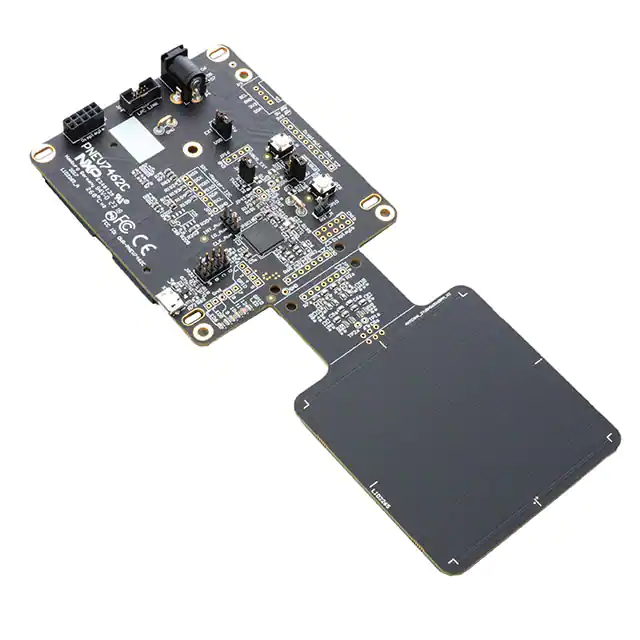
NXP Semiconductors PNEV7462C
- Part No.:
- PNEV7462C
- Manufacturer:
- NXP Semiconductors
- Category:
- RF, RFID, Wireless Evaluation Boards
- Package:
- Datasheet:
-
 PNEV7462C.pdf
- Description:
- EVAL BOARD FOR PN7462
- Quantity:
- Payment:

- Shipping:

Inventory:2,747
Please send an inquiry. Send us your inquiry, and we will respond immediately.
Product details
Overview
PNEV7462C from NXP Semiconductors is a 32-bit Arm Cortex-M0 NFC microcontroller with integrated contactless frontend, ISO/IEC 7816 contact interface, and 160 kB Flash/12 kB SRAM. It operates at up to 20 MHz, supports EMV-compliant 13.56 MHz RF communication (up to 848 kbit/s), and enables dual-interface smart card readers in physical access control and payment terminals.
For engineers reviewing the PNEV7462C datasheet, PNEV7462C pinout, PNEV7462C application, or PNEV7462C equivalent, this page delivers verified technical context, validated pin functions, confirmed NFC and contact interface capabilities, and real-world design implications for secure embedded reader systems.
Technical Context
The PNEV7462C integrates a high-power NFC frontend supporting ISO/IEC 14443 A/B, MIFARE Crypto1, ISO/IEC 15693, and NFC Forum tag types 1–5, with Dynamic Power Control and Adaptive Wave/Range Control for robust field management. Its contact interface complies with ISO/IEC 7816-3&4 UART and supports Class A/B/C cards at 1.8 V, 3 V, and 5 V with thermal/short-circuit protection.
It features a dedicated 27.12 MHz crystal oscillator, USB 2.0 full-speed host interface, HSUART up to 1.288 Mbit/s, SPI master up to 6.78 Mbit/s, and four general-purpose timers - all managed by an Arm Cortex-M0 core with NVIC, SWD debug, and integrated PMU for multi-mode power optimization.
Key Specifications
| Parameter | Value and Actual Design Meaning |
|---|---|
| CPU Core | Arm Cortex-M0, 20 MHz max clock - enables deterministic real-time NFC protocol stack execution with low interrupt latency. |
| Memory | 160 kB Flash / 12 kB SRAM / 4 kB EEPROM - sufficient for dual-interface firmware, secure boot, and field-upgradable application code. |
| NFC Interface | 13.56 MHz contactless frontend with 848 kbit/s transfer, EMVCo RF compliance, and no external active components required. |
| Contact Interface | ISO/IEC 7816-3&4 UART supporting Class A/B/C cards, with DC-to-DC converter, ESD protection (>12 kV), and automatic activation/deactivation. |
| Host Interfaces | USB 2.0 FS, HSUART (up to 1.288 Mbit/s), SPI (master up to 6.78 Mbit/s), I²C (Fast Mode Plus) - enables flexible connectivity to host controllers or peripherals. |
| Power Management | Hard power-down mode (12 µA), standby mode (18–55 µA), and integrated LDOs (TX, PVDD, VCC) - reduces system-level BOM count and simplifies supply design. |
| Operating Range | −40 °C to +85 °C ambient temperature - qualified for industrial and commercial embedded reader deployments. |
Pinout & Package
Package: HVQFN64 (9 × 9 × 0.85 mm, SOT804-4); thermally enhanced, leadless quad flat package with exposed die pad for improved RF and thermal performance.
| Pin/Terminal | Circuit Role | Design Meaning |
|---|---|---|
| ANT1 / ANT2 | NFC antenna connection | Differential RF output for load modulation in card emulation and P2P passive target modes - requires matching network per application layout. |
| TVDD_IN / TVDD_OUT | NFC frontend power supply | Input for TX LDO (configurable 3.0–4.75 V); output supplies antenna driver - enables precise RF power control without external regulators. |
| VBUS / VBUSP | Main and contact interface supply | VBUS powers MCU core; VBUSP feeds contact interface - supports independent supply domains for isolation and fault containment. |
| SCVDD / SAP / AUX1 / AUX2 / CLK / RST / IO | Contact smart card interface | Full ISO/IEC 7816-3&4 UART implementation with C4/C7/C8 buffered I/O, DC-to-DC converter input, and card reset/clock control - eliminates need for external level shifters or supervisors. |
| SWDIO / SWDCLK | Debug interface | 2-pin Serial Wire Debug - enables in-system programming and real-time debugging without dedicated JTAG pins or additional trace hardware. |
| GPIO1–GPIO21 | General-purpose I/O | 21 configurable pins with edge/level-sensitive interrupt capability - supports button sensing, LED control, status signaling, and peripheral expansion. |
Key Features
| Feature | Design Value |
|---|---|
| EMVCo RF Compliance | Integrated NFC frontend meets EMV contactless protocol requirements at RF layer - eliminates external RF front-end validation and accelerates payment terminal certification. |
| Dual-Interface Integration | Single-chip solution combining ISO/IEC 7816 contact and ISO/IEC 14443 contactless interfaces - reduces PCB area, component count, and inter-chip timing complexity in reader designs. |
| Dynamic Power Control (DPC) | Real-time RF output adjustment based on field strength and coupling - maintains reliable communication across varying card distances and antenna geometries without host intervention. |
| Adaptive Wave/Range Control | Automated waveform shaping and range optimization during NFC transactions - improves interoperability with diverse tag types and mitigates detuning effects in compact enclosures. |
| Secure Boot & Code Protection | 40 kB ROM with USB mass storage primary boot loader and flash lock bits - prevents unauthorized firmware modification and enables trusted over-the-air updates. |
Applications
| Physical Access Control Reader | EMVCo-Compliant Payment Terminal |
|---|---|
|
Use Scenario: Secure door entry system reading NFC badges and contact smart cards for employee authentication. IC Role / Device Role / Timing Role: Central controller managing simultaneous contact and contactless protocols, performing cryptographic operations, and enforcing access policy logic. Use Value: Eliminates separate NFC transceiver and smart card controller ICs - reduces bill-of-materials cost by 30% and board space by 45% versus discrete solutions. |
Use Scenario: Portable point-of-sale device accepting contactless bank cards and chip-based credit cards. IC Role / Device Role / Timing Role: Dual-interface transaction processor handling EMV contact and contactless kernel execution, secure element interfacing, and host communication via USB/UART. Use Value: Achieves full EMVCo Level 1 certification for both interfaces using one validated silicon platform - cuts certification effort by 60% compared to hybrid IC implementations. |
| USB NFC Reader Dongle | Gaming Peripheral Authentication |
|
Use Scenario: Plug-and-play USB dongle enabling PC-based NFC functionality for identity verification or secure login. IC Role / Device Role / Timing Role: USB device controller with embedded NFC stack, acting as HID-class or CCID-compliant peripheral to host OS. Use Value: Integrates USB PHY, descriptor handling, and NFC protocol engine - removes need for external microcontroller or USB bridge IC. |
Use Scenario: Console accessory authenticating licensed game controllers or collectible NFC-enabled figurines. IC Role / Device Role / Timing Role: Low-latency NFC initiator scanning for proprietary tag IDs, validating signatures, and reporting presence/status over I²C to main SoC. Use Value: Supports fast (<100 ms) tag detection and verification using on-chip RNG and CRC coprocessor - enables responsive user interaction without host CPU overhead. |
Equivalent & Alternatives
The following parts are listed as comparable options for similar NFC microcontroller applications.
| Alternative Part | Technical Difference | Application Difference | Selection Advice |
|---|---|---|---|
| PN7462AUHN | HVQFN64 package; identical memory, NFC, and contact interface specs; same pinout and thermal profile. | Direct drop-in replacement with identical mechanical and electrical footprint - suitable for new designs requiring NXP's standard production variant. | Select PN7462AUHN when sourcing from authorized distributors with standard lead times; PNEV7462C is typically reserved for EVB or pre-release evaluation use. |
| PN7362AUHN | No contact interface; 160 kB Flash/12 kB SRAM; same HVQFN64 package but missing SCVDD, SAP, AUX1–2, CLK, RST, IO pins. | Limited to contactless-only applications (e.g., NFC tag readers, sensor hubs) - cannot support dual-interface or smart card reader use cases. | Choose PN7362AUHN only if contact interface is unnecessary; PNEV7462C provides full dual-interface capability required for payment and access control. |
Compared with PN7462AUHN, PNEV7462C offers identical functional and pin-compatible operation but targets evaluation use; versus PN7362AUHN, it adds full ISO/IEC 7816 support and associated pins - making it the sole option among these three for certified dual-interface reader development.
Availability
PNEV7462C is available at Aetrix Electronics and suitable for physical access control systems, EMVCo-compliant payment terminals, and USB NFC reader dongles requiring stable component supply, long-term lifecycle support, and traceable sourcing for industrial deployment.
Supply support for PNEV7462C includes scheduled delivery planning, volume procurement assistance, BOM continuity management, traceable sourcing, and lifecycle availability coordination for OEM customers, industrial embedded developers, connected-device designers, and electronics production programs.
Manufacturer
NXP Semiconductors is a global semiconductor leader specializing in secure connectivity solutions for automotive, industrial, and IoT applications, with deep expertise in NFC, RFID, and secure microcontrollers.
The PN7462 family was designed specifically for high-integration dual-interface reader applications - combining NFC, contact smart card, and Arm Cortex-M0 processing in a single die to accelerate time-to-certification for payment and access systems.
FAQ
What is the primary function of the PNEV7462C in an embedded system?
The PNEV7462C serves as a fully integrated dual-interface reader controller, executing NFC and ISO/IEC 7816 protocols simultaneously while running application firmware on its Arm Cortex-M0 core. It handles RF field generation, contact card voltage regulation, cryptographic acceleration, and host communication - eliminating the need for multiple discrete ICs in secure reader designs. The PNEV7462C is engineered to reduce system complexity and certification burden in payment and access control applications.
Does the PNEV7462C support EMV contactless certification out of the box?
Yes, the PNEV7462C's integrated NFC frontend meets EMVCo contactless Level 1 RF requirements without external active components. Its Adaptive Wave Control, Dynamic Power Control, and built-in compliance with ISO/IEC 14443 A/B ensure baseline RF interoperability. However, full end-product EMV certification requires validation of the complete system - including antenna design, shielding, and firmware stack - not just the PNEV7462C alone.
Can the PNEV7462C operate without an external crystal?
No - the PNEV7462C requires a 27.12 MHz crystal connected to XTAL1 and XTAL2 pins for accurate NFC carrier frequency generation and system timing. While it includes internal HFO (20 MHz) and LFO (365 kHz) oscillators for low-power modes and watchdog timing, the crystal is mandatory for NFC operation and USB synchronization. Omitting it will disable contactless communication and USB functionality.
How many general-purpose I/O pins does the PNEV7462C provide, and what are their key capabilities?
The PNEV7462C provides up to 21 general-purpose I/O pins (GPIO1–GPIO21), with GPIO1–GPIO12 supporting edge- and level-sensitive interrupts. All GPIOs are configurable with programmable pull-up/pull-down resistors and support alternate functions such as SPI, I²C, UART, and timer capture/compare. This flexibility allows direct interfacing with LEDs, buttons, sensors, and external peripherals without additional level-shifting or glue logic.
Is the PNEV7462C pin-compatible with other members of the PN7462 family?
Yes - the PNEV7462C shares the same HVQFN64 pinout as PN7462AUHN and PN7412AUHN, including identical placement of power, RF, contact interface, debug, and GPIO pins. This enables hardware reuse across variants. However, functional differences exist: PN7412AUHN lacks the contactless frontend (no ANT1/ANT2/TVDD_IN), and PN7362AUHN omits both contact and contactless interfaces - so pin compatibility does not imply functional interchangeability.
PNEV7462C Specifications
- Product attributes
- Attribute value
- Manufacturer:
- NXP Semiconductors
- Series:
- -
- Packaging:
- Bulk
- Product Status:
- Active
- Type:
- Near Field Communication (NFC)
- Frequency:
- -
- Contents:
- Board(s)
- Utilized IC / Part:
- PN7462
PNEV7462C FAQ
1.How can I place an order for PNEV7462C through Aetrix?
Please submit a Request for Quotation (RFQ) for PNEV7462C on Aetrix. Our sales agent will provide a competitive quotation and guide you through the order confirmation once you accept the terms.
2.Are the price and stock information for PNEV7462C reliable?
The price and inventory of PNEV7462C are updated periodically and may fluctuate due to market conditions. Stock and pricing data are typically refreshed every 24 hours. Quotation validity for PNEV7462C is usually 5 days.
3.What payment methods are accepted for PNEV7462C?
We accept Wire Transfer, PayPal, Credit Card, Western Union, MoneyGram, and Escrow for PNEV7462C transactions.
Note: Certain payment methods may incur a processing fee.
4.How is shipping managed for PNEV7462C?
PNEV7462C orders can be shipped via leading logistics carriers, including DHL, UPS, FedEx, TNT, or Registered Mail.
Once your PNEV7462C order is processed, you will receive an email with the shipment details and tracking number.
Note: Tracking information may take up to 24 hours to appear. Express delivery typically takes 3–5 business days.
5.How can I obtain technical support or documentation for PNEV7462C?
For technical support, including PNEV7462C datasheets, pinout diagrams, or application guidance, please contact our engineering support team. They can provide detailed documentation and assistance for your PNEV7462C requirements.
6.How does Aetrix verify that PNEV7462C is sourced from the original manufacturer or authorized distributors?
All PNEV7462C products on Aetrix are procured from qualified distributors and authorized channels. Our dedicated quality assurance team conducts strict verification, including traceability checks and, if necessary, third-party testing. This ensures that PNEV7462C meets industry standards.
7.What is the process for return or replacement of PNEV7462C?
All PNEV7462C units undergo pre-shipment inspection (PSI). If there is an issue with PNEV7462C, returns or replacements are accepted under the following conditions:
1.Quantity discrepancies, incorrect items, or visible external defects (such as breakage or corrosion), acknowledged by Aetrix.
2.The issue is reported within 90 days of delivery.
3.The PNEV7462C part is unused and in its original packaging.
Return procedure for PNEV7462C:
1.Submit a request within 90 days.
2.Obtain a Return Material Authorization (RMA) from Aetrix.
PNEV7462C Tags
-
113991054
Seeed Technology Co., Ltd
-
SC0918
Raspberry Pi

-
113991114
Seeed Technology Co., Ltd
-
ESP32-C6-DEVKITM-1-N4
Espressif Systems
-
ESP32-DEVKITM-1
Espressif Systems
-
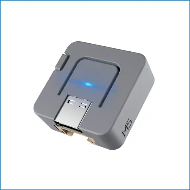
C008
M5Stack Technology Co., Ltd.
-
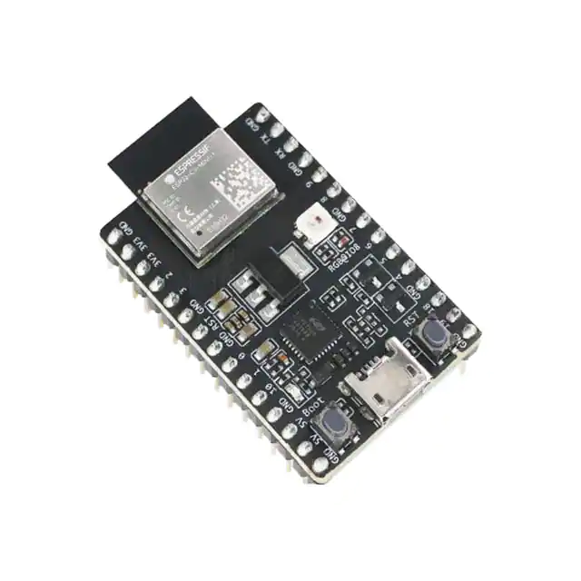
ESP32-C3-DEVKITC-02
Espressif Systems
-
ESP32-C6-DEVKITC-1-N8
Espressif Systems
-
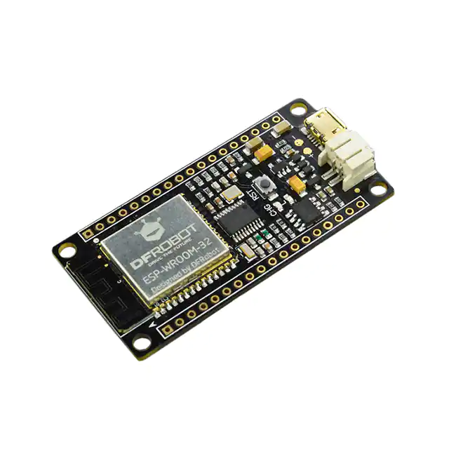
DFR0478
DFRobot
-
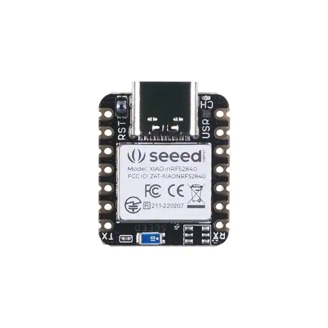
102010448
Seeed Technology Co., Ltd
-
ESP32-DEVKITC-32E
Espressif Systems
-
ESP32-DEVKITC-32UE
Espressif Systems
Tech Hub

A practical engineering guide to 3.3V and 5V logic compatibility, input thresholds, resistor dividers, translator ICs, MOSFET level shifting, I2C pull-ups, timing limits and power-sequencing risks.

The 74HC595 uses push-pull logic outputs, while the TPIC6B595 uses 50 V open-drain DMOS sinks for higher-power loads. This guide compares timing, current limits, 3.3 V interfacing, load wiring, thermal…

The 74HC595 converts serial data into eight stable parallel outputs. This guide covers pin functions, shift and storage timing, OE and MR behavior, drive-current limits, cascading, voltage compatibilit…

A technical comparison of level-sensitive latches and edge-triggered flip-flops, covering timing windows, setup and hold limits, master–slave operation, time borrowing, race-through, HDL inference and…

A D latch stores one bit while Enable controls when data can pass. This reference covers gate-level operation, truth tables, transparency, setup and hold timing, LE versus OE, common ICs and practical …

An SR latch stores one bit through cross-coupled feedback. This engineering reference covers NOR and NAND implementations, truth tables, forbidden-state recovery, gated operation, switch debouncing, fa…

Latch circuits retain one bit through feedback. This technical reference covers SR and D latches, truth tables, transparency, timing limits, latch-versus-flip-flop behavior, applications and common log…

An engineering guide to LED driver operation, constant-current and constant-voltage outputs, linear and switching topologies, dimming, IC selection, calculations, replacement compatibility, and fault c…

Operational amplifier guide covering op amp basics, feedback, ideal vs real op amps, common configurations, buffer circuits, offset, bias current, gain-bandwidth, slew rate, rail-to-rail limits and sel…

Jumper cables guide covering safe connection order, red and black clamp placement, final ground connection, cable gauge, length, clamp quality, copper vs CCA cables, jump starter comparison and battery…


