
 My Inquiry
 My Account


Renesas PS9307AL-AX
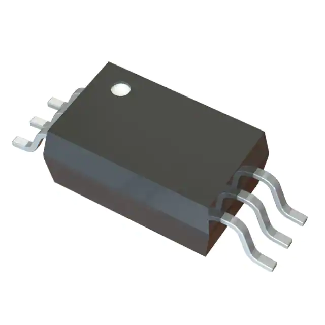
- Part No.:
- PS9307AL-AX
- Manufacturer:
- Renesas
- Category:
- Isolators - Gate Drivers
- Package:
- 6-SOIC (0.268", 6.80mm Width)
- Datasheet:
-
 PS9307AL-AX.pdf
- Description:
- OPTOISO 5KV 1CH GATE DVR 6SDIP
- Quantity:
- Payment:

- Shipping:

Inventory:1,476
Please send an inquiry. Send us your inquiry, and we will respond immediately.
Product details
Overview
PS9307AL-AX from Renesas Electronics is a 6-pin SDIP surface-mount photocopler optimized for IGBT and power MOSFET gate driving, featuring 0.6 A peak output current, ±50 kV/µs common-mode transient immunity (CMR), and 150 ns max propagation delay (tPLH/tPHL). It integrates an AlGaAs LED input stage with on-chip photodiode, signal processing circuitry, and power MOSFET output stage, and operates across −40 °C to +125 °C ambient temperature.
For engineers reviewing the PS9307AL-AX datasheet, PS9307AL-AX pinout, PS9307AL-AX application, or PS9307AL-AX equivalent, this device is selected for high-reliability industrial inverter and AC servo gate drive circuits where high-speed isolation, reinforced insulation, and robust noise immunity are required.
Technical Context
The PS9307AL-AX implements optical coupling between input LED and output power MOSFETs via integrated photodiode and signal conditioning circuitry, enabling galvanic isolation up to 5,000 Vr.m.s.. Its UVLO circuit triggers at 8.6–9.8 V (rising) and 6.8–8.2 V (falling), with 0.4 V hysteresis, ensuring stable gate drive under supply fluctuations.
Designed for high-CMR operation, it achieves ≥±50 kV/µs immunity at both high- and low-level outputs under 1.5 kV common-mode step, with propagation delay matching ≤±80 ns between units. The gull-wing leaded SDIP package provides 7 mm creepage distance and supports infrared reflow soldering up to 260 °C peak.
Key Specifications
| Parameter | Value and Actual Design Meaning |
|---|---|
| Peak Output Current | 0.6 A MAX - sufficient to drive medium-power IGBTs (e.g., 30–60 A rated) with fast turn-on/turn-off |
| Propagation Delay | 150 ns MAX (tPLH/tPHL) - enables switching at up to 250 kHz with minimal timing skew |
| CMR | ±50 kV/µs MIN - suppresses false triggering in noisy motor-drive environments with rapid bus transients |
| Operating Temperature | −40 °C to +125 °C - supports under-hood and industrial enclosure deployments without derating |
| Isolation Voltage | 5,000 Vr.m.s. - meets reinforced insulation requirements per UL1577, CSA C22.2 No.62368-1, EN 62368-1 |
| Supply Voltage Range | 10 V to 30 V - compatible with standard 12 V and 24 V gate drive rails |
| UVLO Threshold | 8.6–9.8 V (rising), 6.8–8.2 V (falling) - prevents partial turn-on of power devices during brownout conditions |
Pinout & Package
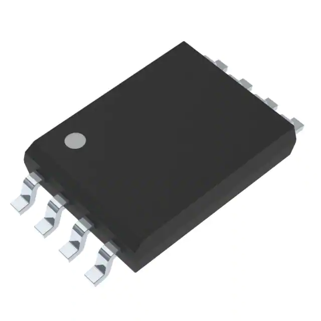
PS9307AL-AX uses a 6-pin Shrink Dual In-line Package (SDIP) with gull-wing surface-mount leads, 9.7 mm × 3.7 mm footprint, 0.27 g typical weight, and 7 mm minimum creepage distance. Mount pad dimensions: A = 9.2 mm, B = 1.27 mm, C = 0.8 mm, D = 2.2 mm.
| Pin/Terminal | Circuit Role | Design Meaning |
|---|---|---|
| 1. Anode | LED input anode | Connects to current-limited forward bias source; requires ≤12 mA IF for reliable switching |
| 2. NC | No connection | Must be left open or tied to GND on LED side; not usable as signal path or bypass |
| 3. Cathode | LED input cathode | Completes LED forward path; reverse voltage limited to 5 V |
| 4. GND | Output-side ground reference | Return for VO and VCC; must be low-impedance and decoupled with ≥1 µF capacitor within 10 mm |
| 5. VO | Output driver source terminal | Delivers 0.6 A peak to IGBT/MOSFET gate; voltage swing 0 to VCC |
| 6. VCC | Output-side supply rail | Accepts 10–30 V; powers internal MOSFETs and logic; UVLO monitors this node |
Key Features
| Feature | Design Value |
|---|---|
| Reinforced insulation certification | UL1577 (double protection), CSA C22.2 No.62368-1, EN 62368-1 - enables safety-critical motor control designs without external isolation barriers |
| Integrated UVLO with hysteresis | 8.6–9.8 V rising threshold, 0.4 V hysteresis - eliminates gate oscillation during marginal supply conditions |
| High-speed switching | 100 ns typical tPLH/tPHL, 5 ns typical rise/fall time - supports >200 kHz PWM in servo inverters |
| Pb-free construction | Ni/Pd/Au plating, RoHS-compliant - meets global environmental compliance requirements for industrial manufacturing |
| Thermal robustness | Rated for continuous operation at +125 °C ambient - eliminates need for heatsinking in compact drives |
Applications
| Industrial Inverter | AC Servo Drive |
|---|---|
|
Use Scenario: Three-phase motor control in HVAC compressors and pump systems using 600 V IGBT modules. IC Role / Device Role / Timing Role: Isolated gate driver providing level-shifted, noise-immune turn-on/turn-off signals to upper- and lower-leg IGBTs. Use Value: ±50 kV/µs CMR prevents false triggering during 1.5 kV bus transients, ensuring safe shoot-through prevention. |
Use Scenario: High-bandwidth position control in CNC machine tool spindles with 20 kHz PWM switching. IC Role / Device Role / Timing Role: Fast, isolated gate driver delivering precise 100 ns timing margins to SiC MOSFET half-bridges. Use Value: 150 ns max propagation delay ensures <1% timing error at 20 kHz, maintaining vector control accuracy. |
| Solar MPPT Inverter | EV Onboard Charger |
|
Use Scenario: DC-DC stage in grid-tied solar inverters using 1200 V IGBTs with fast dv/dt edges. IC Role / Device Role / Timing Role: Isolated gate driver interfacing microcontroller PWM outputs to high-side IGBT gates. Use Value: 5,000 Vr.m.s. isolation withstands system-level surge testing per IEC 61000-4-5, supporting Class III installations. |
Use Scenario: Bidirectional AC/DC conversion in 6.6 kW EV onboard chargers operating at 100 kHz switching frequency. IC Role / Device Role / Timing Role: Compact, thermally efficient gate driver for GaN HEMT half-bridge stages. Use Value: −40 °C to +125 °C rating allows direct mounting on power board near magnetics, reducing parasitic inductance. |
Equivalent & Alternatives
The following parts are listed as comparable options for similar IGBT gate driver applications.
| Alternative Part | Technical Difference | Application Difference | Selection Advice |
|---|---|---|---|
| TLP350(D,F) | 0.5 A peak output, 100 ns max tPLH/tPHL, 3750 Vr.m.s. isolation, no integrated UVLO | Lacks UVLO and lower CMR (±35 kV/µs); suitable only for lower-noise, lower-voltage (<600 V) inverters | Select when cost sensitivity outweighs need for reinforced insulation and full UVLO protection |
| ACPL-332J | 0.6 A peak output, 200 ns max tPLH/tPHL, 5000 Vr.m.s., ±35 kV/µs CMR, integrated UVLO | Slower propagation, lower CMR, and wider SO-6 package (10.3 mm × 3.9 mm vs. 9.7 mm × 3.7 mm) | Choose when board space permits larger footprint and system noise is below 35 kV/µs |
Compared with TLP350(D,F) and ACPL-332J, PS9307AL-AX delivers superior noise immunity (±50 kV/µs), tighter timing control (150 ns max delay), and smaller SDIP footprint-making it optimal for space-constrained, high-dv/dt industrial drives requiring reinforced safety certification.
Availability
PS9307AL-AX is available at Aetrix Electronics and suitable for industrial inverter, AC servo drive, and solar MPPT converter applications requiring stable component supply, long-term lifecycle support, and certified reinforced insulation.
Supply support for PS9307AL-AX includes scheduled delivery planning, volume procurement assistance, BOM continuity management, traceable sourcing, and lifecycle availability coordination for OEM customers, industrial embedded developers, connected-device designers, and electronics production programs.
Manufacturer
Renesas Electronics is a global semiconductor leader specializing in microcontrollers, analog, power, and connectivity solutions for industrial, automotive, and infrastructure markets.
The PS9307AL-AX belongs to Renesas' high-CMR photocopler product line, engineered specifically for robust gate driving in harsh electrical environments such as motor drives and renewable energy systems.
FAQ
What is the maximum recommended forward current for the PS9307AL-AX LED input?
The PS9307AL-AX specifies a recommended forward current of 8–12 mA (IF(ON)) under normal operation. Absolute maximum forward current is 25 mA continuous, but peak transient current up to 1.0 A is allowed for pulses <1 µs. Exceeding 12 mA continuously reduces LED lifetime and increases power dissipation beyond the 45 mW diode rating.
Does the PS9307AL-AX include undervoltage lockout (UVLO) functionality?
Yes, the PS9307AL-AX integrates a dedicated UVLO circuit that monitors the VCC pin. It asserts output disable when VCC falls below 6.8–8.2 V (falling threshold) and re-enables output when VCC rises above 8.6–9.8 V (rising threshold), with 0.4 V hysteresis. This prevents partial turn-on of connected IGBTs or MOSFETs during supply brownouts.
Can Pin 2 (NC) on the PS9307AL-AX be used as a ground connection?
Pin 2 is explicitly designated as NC (No Connection) in the PS9307AL-AX datasheet. It may be left unconnected or tied to GND on the LED side-but must never be used as a signal path, bypass node, or current return. Using it otherwise risks degrading internal noise immunity and violating isolation integrity.
What is the creepage distance specification for the PS9307AL-AX package?
The PS9307AL-AX has a minimum creepage distance of 7 mm and minimum air distance of 7 mm, as confirmed in the R08DS0122EJ0101 datasheet. This meets reinforced insulation requirements for basic functional safety in industrial equipment operating up to 300 V RMS working voltage per IEC 62368-1.
Is the PS9307AL-AX compliant with RoHS and lead-free assembly standards?
Yes, the PS9307AL-AX is a Pb-free product with Ni/Pd/Au solder plating, compliant with EU RoHS Directive 2011/65/EU. It supports infrared reflow soldering with peak package temperature ≤260 °C for ≤10 seconds, and is qualified for three reflow cycles per JEDEC J-STD-020.
PS9307AL-AX Specifications
- Product attributes
- Attribute value
- Manufacturer:
- Renesas
- Series:
- -
- Package/Case:
- 6-SOIC (0.268", 6.80mm Width)
- Packaging:
- Strip
- Product Status:
- Active
- Technology:
- Optical Coupling
- Number of Channels:
- 1
- Voltage - Isolation:
- 5000Vrms
- Common Mode Transient Immunity (Min):
- 50kV/µs
- Propagation Delay tpLH / tpHL (Max):
- 150ns, 150ns
- Pulse Width Distortion (Max):
- 50ns
- Rise / Fall Time (Typ):
- 6ns, 7ns
- Current - Output High, Low:
- 400mA, 400mA
- Current - Peak Output:
- 600mA
- Voltage - Forward (Vf) (Typ):
- 1.56V
- Current - DC Forward (If) (Max):
- 25 mA
- Voltage - Output Supply:
- 10V ~ 30V
- Grade:
- -
- Qualification:
- -
- Operating Temperature:
- -40°C ~ 125°C
- Mounting Type:
- Surface Mount
- Supplier Device Package:
- 6-SDIP
- Approval Agency:
- CSA, UL, VDE
PS9307AL-AX FAQ
1.How can I place an order for PS9307AL-AX through Aetrix?
Please submit a Request for Quotation (RFQ) for PS9307AL-AX on Aetrix. Our sales agent will provide a competitive quotation and guide you through the order confirmation once you accept the terms.
2.Are the price and stock information for PS9307AL-AX reliable?
The price and inventory of PS9307AL-AX are updated periodically and may fluctuate due to market conditions. Stock and pricing data are typically refreshed every 24 hours. Quotation validity for PS9307AL-AX is usually 5 days.
3.What payment methods are accepted for PS9307AL-AX?
We accept Wire Transfer, PayPal, Credit Card, Western Union, MoneyGram, and Escrow for PS9307AL-AX transactions.
Note: Certain payment methods may incur a processing fee.
4.How is shipping managed for PS9307AL-AX?
PS9307AL-AX orders can be shipped via leading logistics carriers, including DHL, UPS, FedEx, TNT, or Registered Mail.
Once your PS9307AL-AX order is processed, you will receive an email with the shipment details and tracking number.
Note: Tracking information may take up to 24 hours to appear. Express delivery typically takes 3–5 business days.
5.How can I obtain technical support or documentation for PS9307AL-AX?
For technical support, including PS9307AL-AX datasheets, pinout diagrams, or application guidance, please contact our engineering support team. They can provide detailed documentation and assistance for your PS9307AL-AX requirements.
6.How does Aetrix verify that PS9307AL-AX is sourced from the original manufacturer or authorized distributors?
All PS9307AL-AX products on Aetrix are procured from qualified distributors and authorized channels. Our dedicated quality assurance team conducts strict verification, including traceability checks and, if necessary, third-party testing. This ensures that PS9307AL-AX meets industry standards.
7.What is the process for return or replacement of PS9307AL-AX?
All PS9307AL-AX units undergo pre-shipment inspection (PSI). If there is an issue with PS9307AL-AX, returns or replacements are accepted under the following conditions:
1.Quantity discrepancies, incorrect items, or visible external defects (such as breakage or corrosion), acknowledged by Aetrix.
2.The issue is reported within 90 days of delivery.
3.The PS9307AL-AX part is unused and in its original packaging.
Return procedure for PS9307AL-AX:
1.Submit a request within 90 days.
2.Obtain a Return Material Authorization (RMA) from Aetrix.
PS9307AL-AX Tags
.JPG)
-
TLP152(TPL,E
Toshiba Semiconductor and Storage

-
HT0740LG-G
Microchip Technology
-
FOD8314TR2
onsemi
-
1EDI60N12AFXUMA1
Infineon Technologies
-
1EDB7275FXUMA1
Infineon Technologies
-
UCC5350MCDR
Texas Instruments

-
2EDB7259KXUMA1
Infineon Technologies

-
UCC5304DWVR
Texas Instruments
-
SI8261BBC-C-ISR
Skyworks Solutions Inc.
-
HT0440LG-G
Microchip Technology
-
HCPL-0302-500E
Broadcom Limited
-
STGAP2HSCMTR
STMicroelectronics
Tech Hub

TTL and CMOS logic families differ in thresholds, loading, output drive, power and timing. This engineering guide compares 74HC and 74HCT, calculates noise margins and checks 3.3 V/5 V compatibility.

A practical engineering guide to 3.3V and 5V logic compatibility, input thresholds, resistor dividers, translator ICs, MOSFET level shifting, I2C pull-ups, timing limits and power-sequencing risks.

The 74HC595 uses push-pull logic outputs, while the TPIC6B595 uses 50 V open-drain DMOS sinks for higher-power loads. This guide compares timing, current limits, 3.3 V interfacing, load wiring, thermal…

The 74HC595 converts serial data into eight stable parallel outputs. This guide covers pin functions, shift and storage timing, OE and MR behavior, drive-current limits, cascading, voltage compatibilit…

A technical comparison of level-sensitive latches and edge-triggered flip-flops, covering timing windows, setup and hold limits, master–slave operation, time borrowing, race-through, HDL inference and…

A D latch stores one bit while Enable controls when data can pass. This reference covers gate-level operation, truth tables, transparency, setup and hold timing, LE versus OE, common ICs and practical …

An SR latch stores one bit through cross-coupled feedback. This engineering reference covers NOR and NAND implementations, truth tables, forbidden-state recovery, gated operation, switch debouncing, fa…

Latch circuits retain one bit through feedback. This technical reference covers SR and D latches, truth tables, transparency, timing limits, latch-versus-flip-flop behavior, applications and common log…

An engineering guide to LED driver operation, constant-current and constant-voltage outputs, linear and switching topologies, dimming, IC selection, calculations, replacement compatibility, and fault c…

Operational amplifier guide covering op amp basics, feedback, ideal vs real op amps, common configurations, buffer circuits, offset, bias current, gain-bandwidth, slew rate, rail-to-rail limits and sel…


