
 My Inquiry
 My Account


NXP Semiconductors PTN3363BSMP
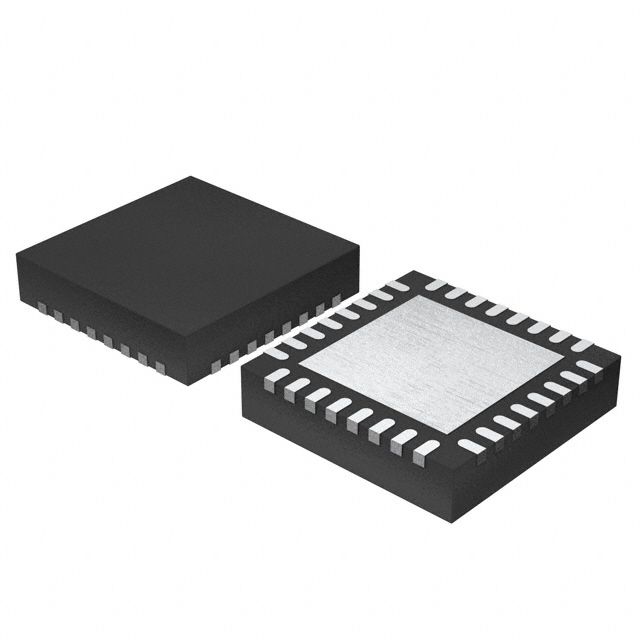
- Part No.:
- PTN3363BSMP
- Manufacturer:
- NXP Semiconductors
- Category:
- Specialized
- Package:
- 32-VFQFN Exposed Pad
- Datasheet:
-
 PTN3363BSMP.pdf
- Description:
- IC INTFACE SPECIALIZED 32HVQFN
- Quantity:
- Payment:

- Shipping:

Inventory:3,309
Please send an inquiry. Send us your inquiry, and we will respond immediately.
Product details
Overview
PTN3363BSMP from NXP Semiconductors is a low-power HDMI/DVI level shifter IC that converts four lanes of low-swing AC-coupled differential inputs to DVI v1.0 and HDMI v1.4b–compliant TMDS outputs at up to 3.4 Gbit/s per lane, supports 4K × 2K/3D video, integrates active DDC buffering with I²C-level shifting (3.3 V ↔ 5 V), and provides HPD voltage translation (5 V sink → 3.3 V source) for DisplayPort++ adapter applications.
For engineers reviewing the PTN3363BSMP datasheet, PTN3363BSMP pinout, PTN3363BSMP application, or PTN3363BSMP equivalent, key selection considerations include its 32-pin HVQFN package, programmable equalization (0–6 dB), HIZ_EN-controlled input termination, REXT-based current reference accuracy, and back-current-safe sink-side I/Os essential for robust hot-plug and redriver implementations.
Technical Context
The PTN3363BSMP implements transparent, non-retiming level translation across three signal domains: four high-speed TMDS lanes (IN_Dx → OUT_Dx) with self-biasing 50 Ω inputs and open-drain current-steering outputs; a bidirectional DDC channel (SCL/SDA) using active I²C-bus buffer architecture with rise-time acceleration on sink-side ports; and a unidirectional HPD level shifter with integrated 200 kΩ pull-down on HPD_SINK.
Its functional modes are controlled by OE_N (TMDS enable), DDC_EN (DDC enable), HIZ_EN (input termination mode), EQ0/EQ1 (4-level equalization), and DDET (HDMI dongle detection enable), all operating independently without state machines or clocked logic - ensuring deterministic latency and zero configuration overhead.
Key Specifications
| Parameter | Value and Actual Design Meaning |
|---|---|
| Max data rate | 3.4 Gbit/s per lane - supports HDMI v1.4b 36-bit deep color, 4K × 2K, and 3D video transport. |
| Supply voltage | 2.8 V to 3.6 V - single 3.3 V ±10 % rail powers full functionality with 72 mW typical consumption. |
| Input interface | Four self-biasing AC-coupled differential pairs (IN_D1± to IN_D4±) compliant with DisplayPort v1.2a/PCIe v1.1 electrical specs. |
| Output interface | Four open-drain current-steering TMDS outputs (OUT_D1± to OUT_D4±) compliant with DVI v1.0/HDMI v1.4b sink requirements. |
| DDC capability | I²C-bus level shifter supporting 400 kHz clock, 3.3 V ↔ 5 V translation, rise-time acceleration on sink-side SCL/SDA, and slave ROM for HDMI dongle detection. |
| HPD translation | Non-inverting level shift from 0–5 V (sink) to 0–3.3 V (source) with integrated 200 kΩ pull-down on HPD_SINK for reliable plug-detection. |
| Equalization | Programmable 0 dB / 2 dB / 4 dB / 6 dB via EQ0/EQ1 binary inputs - compensates channel loss in long-cable or multi-adapter paths. |
Pinout & Package
PTN3363BSMP is housed in a 5 mm × 5 mm × 0.85 mm HVQFN32 package (SOT617-3) with an exposed thermal pad requiring solder connection to system ground for thermal, electrical, and mechanical integrity.
| Pin/Terminal | Circuit Role | Design Meaning |
|---|---|---|
| IN_D1± to IN_D4± (pins 25–32) | Self-biasing differential inputs | Accept low-swing AC-coupled DP/HDMI-coded signals; internal 50 Ω termination enabled when HIZ_EN = LOW. |
| OUT_D1± to OUT_D4± (pins 9–16) | TMDS current-steering outputs | Drive DVI/HDMI-compliant DC-coupled differential loads terminated to 50 Ω @ 3.3 V; back-current safe when unpowered. |
| HPD_SINK (pin 21), HPD_SOURCE (pin 5) | Hot Plug Detect level shifter | Translates sink-side 0–5 V HPD to source-side 0–3.3 V output; HPD_SINK includes 200 kΩ pull-down for 'no display' detection. |
| SCL_SOURCE/SDA_SOURCE (pins 7,6), SCL_SINK/SDA_SINK (pins 19,20) | Active I²C-bus level shifter | Bi-directional 3.3 V ↔ 5 V DDC translation with rise-time acceleration on sink-side ports and overvoltage tolerance when disabled/unpowered. |
| OE_N (pin 17), DDC_EN (pin 22), HIZ_EN (pin 24) | Functional control inputs | Independent enable/disable of TMDS path, DDC path, and input termination mode - no interlock or sequencing required. |
| REXT (pin 4), EQ0 (pin 8), EQ1 (pin 2), DDET (pin 3) | Analog/feature configuration | REXT sets output current accuracy (12.4 kΩ recommended); EQ0/EQ1 select equalization; DDET enables HDMI dongle detection ROM. |
Key Features
| Feature | Design Value |
|---|---|
| Transparent TMDS level shifting | No retiming, no state machines, zero latency - preserves native timing and protocol integrity for DP++, HDMI, and DVI interoperability. |
| Programmable receive equalization | Four discrete settings (0/2/4/6 dB) via EQ0/EQ1 pins - adapts to varying channel loss in adapter cables or PCB traces without firmware. |
| Back-current-safe sink-side I/Os | Blocks reverse current flow from powered sink into unpowered PTN3363 on all TMDS, DDC, and HPD terminals - eliminates risk of backdrive damage. |
| Integrated DDC rise-time acceleration | Active current-source boost on SCL_SINK/SDA_SINK - enables reliable I²C operation up to 1400 pF bus capacitance while meeting HDMI DDC spec. |
| HDMI dongle detection ROM | On-chip I²C slave memory responding to address 81h with ASCII "DP-HDMI ADAPTOR |
Applications
| PC Graphics Interface | Docking Station Hub |
|---|---|
Use Scenario: Integrating HDMI/DVI output on a multi-mode GPU with DisplayPort-native PHY. IC Role / Device Role / Timing Role: Level shifter converting DP PHY's low-swing AC-coupled outputs to HDMI-compliant TMDS signals while preserving pixel-clock alignment and HDCP handshake integrity. Use Value: Enables single-chip GPU to drive HDMI/DVI monitors without redesigning I/O pads or adding external redrivers - reduces BOM count and layout complexity. | Use Scenario: Adding HDMI output to a USB-C/Thunderbolt docking station with native DP Alt Mode support. IC Role / Device Role / Timing Role: Transparent bridge translating DP++ source signals to HDMI sink, handling HPD negotiation and DDC handshaking across voltage domains. Use Value: Supports 4K × 2K@60 Hz video through compact adapter form factor with guaranteed HDMI compliance and plug-and-play monitor detection. |
| DisplayPort-to-HDMI Adapter | Long-Cable DVI Redriver |
Use Scenario: Active cable or dongle converting DisplayPort source to HDMI display with 3D/Deep Color support. IC Role / Device Role / Timing Role: Full-function level shifter with integrated DDC buffer, HPD translation, and dongle detection ROM for certified HDMI interoperability. Use Value: Meets DisplayPort Interoperability Guidelines by enabling HDMI dongle detection via standard DDC read - satisfies certification requirements for commercial adapters. | Use Scenario: Extending DVI signal reach beyond 15 m using passive cabling in industrial kiosk or digital signage systems. IC Role / Device Role / Timing Role: Native HDMI redriver with HIZ_EN-enabled high-Z inputs and external 50 Ω termination - restores signal integrity without protocol conversion. Use Value: Compensates for attenuation and jitter accumulation in long DVI cables while maintaining backward compatibility with legacy DVI sinks. |
Equivalent & Alternatives
The following parts are listed as comparable options for similar HDMI/DVI level shifting applications.
| Alternative Part | Technical Difference | Application Difference | Selection Advice |
|---|---|---|---|
| TI TPD12S016 | Single-lane HDMI level shifter with integrated ESD protection; lacks DDC buffer, HPD translation, and equalization; max 3.0 Gbit/s. | Targeted at cost-sensitive, single-port HDMI add-ons - not suitable for 4-lane DP++ or 4K/3D use cases. | Select only for basic HDMI output where DDC isolation, multi-lane support, or 3.4 Gbit/s operation are unnecessary. |
| Pericom PI3HDX1204A | 4-lane HDMI redriver with fixed 6 dB equalization; no DDC/HPD functions; requires external level-shifting for control signals. | Designed for native HDMI redriver applications only - cannot translate DP++ source signals or manage DDC/HPD handshakes autonomously. | Choose when interfacing HDMI-only sources and sinks; requires companion logic for HPD/DDC management. |
Compared with TPD12S016 and PI3HDX1204A, PTN3363BSMP uniquely integrates full DP++ level shifting, active DDC buffering, HPD translation, and programmable equalization in one HVQFN32 device - eliminating need for supplemental ICs in adapter and docking designs.
Availability
PTN3363BSMP is available at Aetrix Electronics and suitable for PC motherboard graphics interfaces, USB-C docking stations, DisplayPort-to-HDMI adapters, and industrial DVI redriver systems requiring stable component supply, long-term lifecycle assurance, and automotive-grade reliability validation.
Supply support for PTN3363BSMP includes scheduled delivery planning, volume procurement assistance, BOM continuity management, traceable sourcing, and lifecycle availability coordination for OEM customers, industrial embedded developers, connected-device designers, and electronics production programs.
Manufacturer
NXP Semiconductors is a global semiconductor leader specializing in secure connectivity solutions for automotive, industrial, and consumer applications, with core expertise in interface, power management, and secure MCU technologies.
The PTN3363BSMP belongs to NXP's Display Interface portfolio, engineered specifically to simplify DP++ adapter design by consolidating HDMI/DVI level shifting, DDC buffering, HPD translation, and dongle detection into a single low-power, pin-efficient IC.
FAQ
What is the maximum data rate supported by PTN3363BSMP per TMDS lane?
PTN3363BSMP supports up to 3.4 Gbit/s per lane, enabling transmission of HDMI v1.4b 36-bit deep color, 4K × 2K resolution, and 3D video formats. This corresponds to a 340 MHz TMDS clock frequency and is validated per DVI v1.0 and HDMI v1.4b electrical compliance requirements.
Does PTN3363BSMP require configuration or firmware to operate?
No, PTN3363BSMP operates transparently with no retiming, no state machines, and no software configuration. All functionality - including level shifting, equalization, DDC buffering, and HPD translation - is controlled by hardware pins (OE_N, DDC_EN, EQ0/EQ1, HIZ_EN, DDET). The PTN3363BSMP requires no initialization sequence or driver support.
How does PTN3363BSMP handle back-current protection when the sink is powered but PTN3363BSMP is not?
PTN3363BSMP provides back-current-safe design on all sink-side terminals - TMDS outputs (OUT_Dx), DDC I/Os (SCL_SINK/SDA_SINK), and HPD_SINK. When unpowered, it sinks less than negligible leakage current and blocks reverse current flow from the sink into its VDD rail or upstream source, preventing damage or unintended power-up.
What is the purpose of the REXT pin on PTN3363BSMP, and what resistor value is recommended?
The REXT pin (pin 4) sets the current reference for PTN3363BSMP's TMDS output drivers. For optimal output voltage swing accuracy across voltage and temperature, a 12.4 kΩ ±1 % resistor between REXT and GND is recommended. Direct connection to GND or VDD is allowed but reduces accuracy of VOL, differential swing, and edge timing.
Can PTN3363BSMP be used in both DP++ adapter and native HDMI redriver configurations?
Yes - PTN3363BSMP supports both use cases. In DP++ mode, HIZ_EN = LOW enables internal 50 Ω input termination for low-swing AC-coupled DP signals. In native HDMI redriver mode, HIZ_EN = HIGH places inputs in high-Z, allowing external 50 Ω termination - confirmed in Figure 2 and Section 7.1.4 of the datasheet.
PTN3363BSMP Specifications
- Product attributes
- Attribute value
- Manufacturer:
- NXP Semiconductors
- Series:
- -
- Package/Case:
- 32-VFQFN Exposed Pad
- Packaging:
- Tape & Reel (TR)
- Product Status:
- Obsolete
- Applications:
- HDMI
- Interface:
- -
- Voltage - Supply:
- 3.3V
- Supplier Device Package:
- 32-HVQFN (5x5)
- Grade:
- -
- Qualification:
- -
- Mounting Type:
- Surface Mount
PTN3363BSMP FAQ
1.How can I place an order for PTN3363BSMP through Aetrix?
Please submit a Request for Quotation (RFQ) for PTN3363BSMP on Aetrix. Our sales agent will provide a competitive quotation and guide you through the order confirmation once you accept the terms.
2.Are the price and stock information for PTN3363BSMP reliable?
The price and inventory of PTN3363BSMP are updated periodically and may fluctuate due to market conditions. Stock and pricing data are typically refreshed every 24 hours. Quotation validity for PTN3363BSMP is usually 5 days.
3.What payment methods are accepted for PTN3363BSMP?
We accept Wire Transfer, PayPal, Credit Card, Western Union, MoneyGram, and Escrow for PTN3363BSMP transactions.
Note: Certain payment methods may incur a processing fee.
4.How is shipping managed for PTN3363BSMP?
PTN3363BSMP orders can be shipped via leading logistics carriers, including DHL, UPS, FedEx, TNT, or Registered Mail.
Once your PTN3363BSMP order is processed, you will receive an email with the shipment details and tracking number.
Note: Tracking information may take up to 24 hours to appear. Express delivery typically takes 3–5 business days.
5.How can I obtain technical support or documentation for PTN3363BSMP?
For technical support, including PTN3363BSMP datasheets, pinout diagrams, or application guidance, please contact our engineering support team. They can provide detailed documentation and assistance for your PTN3363BSMP requirements.
6.How does Aetrix verify that PTN3363BSMP is sourced from the original manufacturer or authorized distributors?
All PTN3363BSMP products on Aetrix are procured from qualified distributors and authorized channels. Our dedicated quality assurance team conducts strict verification, including traceability checks and, if necessary, third-party testing. This ensures that PTN3363BSMP meets industry standards.
7.What is the process for return or replacement of PTN3363BSMP?
All PTN3363BSMP units undergo pre-shipment inspection (PSI). If there is an issue with PTN3363BSMP, returns or replacements are accepted under the following conditions:
1.Quantity discrepancies, incorrect items, or visible external defects (such as breakage or corrosion), acknowledged by Aetrix.
2.The issue is reported within 90 days of delivery.
3.The PTN3363BSMP part is unused and in its original packaging.
Return procedure for PTN3363BSMP:
1.Submit a request within 90 days.
2.Obtain a Return Material Authorization (RMA) from Aetrix.
PTN3363BSMP Tags

-
NVT4857UKAZ
NXP Semiconductors

-
TCA8418RTWR
Texas Instruments

-
PCA9546APWR
Texas Instruments

-
MD0100N8-G
Microchip Technology

-
PCA9548APW,118
NXP Semiconductors

-
PCA9540BDP,118
NXP Semiconductors

-
PCA9548APWR
Texas Instruments

-
PCA9546APW,118
NXP Semiconductors

-
PTN3360DBS,518
NXP Semiconductors

-
PCA9546ABS,118
NXP Semiconductors

-
PCA9518PWR
Texas Instruments

-
PCA9545APW,118
NXP Semiconductors
Tech Hub

A practical engineering guide to 3.3V and 5V logic compatibility, input thresholds, resistor dividers, translator ICs, MOSFET level shifting, I2C pull-ups, timing limits and power-sequencing risks.

The 74HC595 uses push-pull logic outputs, while the TPIC6B595 uses 50 V open-drain DMOS sinks for higher-power loads. This guide compares timing, current limits, 3.3 V interfacing, load wiring, thermal…

The 74HC595 converts serial data into eight stable parallel outputs. This guide covers pin functions, shift and storage timing, OE and MR behavior, drive-current limits, cascading, voltage compatibilit…

A technical comparison of level-sensitive latches and edge-triggered flip-flops, covering timing windows, setup and hold limits, master–slave operation, time borrowing, race-through, HDL inference and…

A D latch stores one bit while Enable controls when data can pass. This reference covers gate-level operation, truth tables, transparency, setup and hold timing, LE versus OE, common ICs and practical …

An SR latch stores one bit through cross-coupled feedback. This engineering reference covers NOR and NAND implementations, truth tables, forbidden-state recovery, gated operation, switch debouncing, fa…

Latch circuits retain one bit through feedback. This technical reference covers SR and D latches, truth tables, transparency, timing limits, latch-versus-flip-flop behavior, applications and common log…

An engineering guide to LED driver operation, constant-current and constant-voltage outputs, linear and switching topologies, dimming, IC selection, calculations, replacement compatibility, and fault c…

Operational amplifier guide covering op amp basics, feedback, ideal vs real op amps, common configurations, buffer circuits, offset, bias current, gain-bandwidth, slew rate, rail-to-rail limits and sel…

Jumper cables guide covering safe connection order, red and black clamp placement, final ground connection, cable gauge, length, clamp quality, copper vs CCA cables, jump starter comparison and battery…


