
 My Inquiry
 My Account


NXP Semiconductors PTN3460BS/F1,518
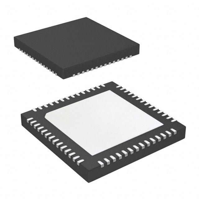
- Part No.:
- PTN3460BS/F1,518
- Manufacturer:
- NXP Semiconductors
- Category:
- Specialized
- Package:
- 56-VFQFN Exposed Pad
- Datasheet:
-
 PTN3460BS/F1,518.pdf
- Description:
- IC INTFACE SPECIALIZED 56HVQFN
- Quantity:
- Payment:

- Shipping:

Inventory:3,079
Please send an inquiry. Send us your inquiry, and we will respond immediately.
Product details
Overview
PTN3460BS/F1,518 from NXP Semiconductors is an embedded DisplayPort (eDP) to LVDS bridge IC that converts high-speed eDP video streams into LVDS signals for driving TFT-LCD panels. It supports 1- or 2-lane eDP input at 1.62 Gbit/s or 2.7 Gbit/s, dual-bus LVDS output up to 112 MHz pixel clock, 24 bpp color depth, and VESA/JEIDA data packing - enabling 1920×1200@60 Hz resolution in notebook and AIO display interfaces.
For engineers reviewing the PTN3460BS/F1,518 datasheet, PTN3460BS/F1,518 pinout, PTN3460BS/F1,518 application, or PTN3460BS/F1,518 equivalent, key selection considerations include eDP v1.2 compliance, on-chip EDID emulation, firmware-configurable LVDS bus routing, programmable pixel clock spreading, and dual-supply (3.3 V/1.8 V) or single-supply (3.3 V only) operation with integrated regulator.
Technical Context
The PTN3460BS/F1,518 implements a full eDP v1.2 receiver with Auto Receive Equalization, Fast/Full Link Training, ASSR authentication, and DPCD register access via AUX channel. Its LVDS transmitter supports dual-bus operation with independent even/odd channel mapping, configurable swing (250–400 mV), center-spread clock modulation (32.9 kHz), and JEIDA/VESA format selection.
System-level control is enabled through three concurrent configuration paths: multi-level hardware pins (CFG1–CFG4), I2C-bus slave interface (100/400 kbit/s), and DP AUX channel. The embedded microcontroller and on-chip NVM allow firmware updates without external memory, while EDID emulation (up to seven structures, v1.3 compliant) eliminates BIOS dependency for panels lacking EDID ROM.
Key Specifications
| Parameter | Value and Actual Design Meaning |
|---|---|
| eDP Compliance | Compliant with DisplayPort v1.2 and eDP v1.2 standards, including ASSR and Enhanced Framing for copy protection. |
| Main Link Rate | 1.62 Gbit/s (RBR) or 2.7 Gbit/s (HBR); supports 1-lane or 2-lane operation with auto-negotiated link training. |
| LVDS Output | Dual-bus mode supports up to 224 mega pixels/sec; single-bus mode up to 112 mega pixels/sec at 25–112 MHz pixel clock. |
| Color Depth & Format | 18 bpp or 24 bpp RGB; supports both VESA and JEIDA data packing formats for panel compatibility. |
| Power Supply | Operates from 3.3 V ±10 % only (internal 1.8 V regulator active) or dual supplies (3.3 V ±10 %, 1.8 V ±5 %). |
| EDID Emulation | On-chip emulation of up to seven distinct EDID v1.3 structures; eliminates need for external EDID ROM or BIOS modification. |
| Operating Temp. | 0 °C to +70 °C ambient; qualified for commercial notebook and AIO platform environments. |
Pinout & Package
HVQFN56 package (7 mm × 7 mm, 0.4 mm pitch) with exposed center pad for thermal relief and electrical grounding. Pin count: 56 terminals; maximum height: 1.0 mm.
| Pin/Terminal | Circuit Role | Design Meaning |
|---|---|---|
| DP0_P / DP0_N | eDP Main Link Lane 0 differential input | AC-coupled inputs for 1.62/2.7 Gbit/s eDP stream; support auto-equalization and link training. |
| AUX_P / AUX_N | eDP AUX channel differential I/O | Carry Native AUX and I2C-over-AUX transactions for DPCD access, EDID reads, and register configuration. |
| LVSAE_P/N – LVSDE_P/N | LVDS even-bus differential outputs | Drive Channel A–D data pairs in even LVDS bus; support channel swapping and polarity inversion. |
| LVSCKE_P / LVSCKE_N | LVDS even-bus clock output | Differential clock signal for even bus; programmable center-spread modulation reduces EMI. |
| PVCCEN / BKLTEN / PWMO | Panel power control outputs | CMOS outputs for panel VCC enable, backlight enable, and PWM dimming - synchronized to video stream timing. |
| RST_N / PD_N | Reset and deep power-down control | Active-low asynchronous reset (RST_N) and hardware-initiated deep power-down (PD_N) for system-level power management. |
Key Features
| Feature | Design Value |
|---|---|
| Embedded microcontroller + NVM | Enables field-upgradable firmware without external memory; supports custom initialization sequences and feature tuning. |
| EDID ROM emulation | Eliminates requirement for external EDID EEPROM or BIOS changes; supports up to seven preloaded EDID v1.3 structures. |
| Programmable LVDS signal swing | Configurable 250/300/400 mV output swing per differential pair to compensate for PCB trace loss or reduce power consumption. |
| LVDS bus and channel routing | Software- or pin-controlled swapping of LVDS buses, channels, and differential pairs - simplifies PCB layout and enables reuse across panel variants. |
| eDP authentication support | Hardware-accelerated Alternate Scrambler Seed Reset (ASSR) and Enhanced Framing for secure content delivery compliance. |
Applications
| Notebook Display Interface | All-in-One (AIO) Platform |
|---|---|
Use Scenario: Integrating high-resolution LCD panels into thin-and-light notebooks using eDP-enabled GPU outputs. IC Role / Device Role / Timing Role: eDP-to-LVDS protocol converter and timing controller; bridges GPU's native eDP output to legacy LVDS panel interface. Use Value: Enables 1920×1200@60 Hz dual-bus LVDS output with zero BIOS EDID dependency and flexible power sequencing. |
Use Scenario: Driving large-format TFT-LCDs in space-constrained AIO desktop systems with eDP-capable chipsets. IC Role / Device Role / Timing Role: High-bandwidth video bridge with embedded timing recovery and panel power coordination. Use Value: Supports dual-supply operation and programmable LVDS swing to match varying panel voltage requirements and trace losses. |
| Netbook / Net Top System | Industrial Panel PC |
Use Scenario: Cost-optimized compact computing platforms requiring low-power, firmware-flexible display connectivity. IC Role / Device Role / Timing Role: Embedded display bridge with on-chip NVM and multi-mode configuration (pins/I2C/AUX). Use Value: Reduces BOM count by eliminating external EDID ROM and timing reference crystal; supports 1-lane eDP for lower-cost designs. |
Use Scenario: Ruggedized panel PCs needing reliable LVDS interface with robust power management and ESD tolerance. IC Role / Device Role / Timing Role: Industrial-grade eDP-to-LVDS bridge with 8 kV HBM ESD rating and 0–70 °C operating range. Use Value: Delivers deterministic panel power-up/down sequencing and deep power-down state for energy-sensitive deployments. |
Equivalent & Alternatives
The following parts are listed as comparable options for similar eDP-to-LVDS bridge applications.
| Alternative Part | Technical Difference | Application Difference | Selection Advice |
|---|---|---|---|
| CH7511B-AB | Supports eDP v1.1 only; no ASSR authentication; requires external EDID ROM; no on-chip NVM for firmware updates. | Limited to legacy eDP sources and panels without advanced copy protection requirements. | Choose when cost sensitivity outweighs firmware flexibility and security compliance needs. |
| PS8408-CRZ | Single-supply only (3.3 V); no dual-bus LVDS mode; max pixel clock 100 MHz; lacks EDID emulation capability. | Suitable for lower-resolution panels (< 1600×900) and simpler power architectures without panel sequencing control. | Prefer when board space is constrained and panel interface requirements are minimal. |
Compared with CH7511B-AB and PS8408-CRZ, the PTN3460BS/F1,518 provides broader eDP v1.2 compliance, on-chip EDID emulation, dual-bus LVDS scalability to 1920×1200@60 Hz, and firmware-upgradable operation - making it optimal for modern notebook, AIO, and industrial panel PC designs requiring security, flexibility, and resolution headroom.
Availability
PTN3460BS/F1,518 is available at Aetrix Electronics and suitable for notebook platforms, all-in-one (AIO) systems, and netbook/net top designs requiring stable component supply, long-term lifecycle support, and firmware-version traceability.
Supply support for PTN3460BS/F1,518 includes scheduled delivery planning, volume procurement assistance, BOM continuity management, traceable sourcing, and lifecycle availability coordination for OEM customers, industrial embedded developers, connected-device designers, and electronics production programs.
Manufacturer
NXP Semiconductors is a global semiconductor company headquartered in Eindhoven, Netherlands, specializing in secure connectivity solutions for automotive, industrial, and consumer electronics.
The PTN3460BS/F1,518 belongs to NXP's display interface product line, engineered specifically to bridge next-generation eDP sources to legacy LVDS panels in space- and power-constrained mobile and embedded platforms.
FAQ
What is the primary function of the PTN3460BS/F1,518?
The PTN3460BS/F1,518 is an embedded DisplayPort (eDP) to LVDS bridge IC that receives eDP video streams from CPUs/GPUs and converts them into LVDS signals compatible with TFT-LCD panels. It handles protocol translation, timing recovery, EDID emulation, and panel power sequencing - enabling seamless integration of modern eDP sources with legacy LVDS displays in notebooks and AIO systems.
Does the PTN3460BS/F1,518 support eDP v1.2 authentication features?
Yes, the PTN3460BS/F1,518 fully supports eDP v1.2 authentication methods including Alternate Scrambler Seed Reset (ASSR) and Enhanced Framing. These features are implemented in hardware to meet content protection requirements for secure video transmission, and are confirmed in the official NXP datasheet Rev. 4 (March 2014).
Can the PTN3460BS/F1,518 operate with only a 3.3 V supply?
Yes, the PTN3460BS/F1,518 can operate using a single 3.3 V ±10 % supply, with its internal regulator generating the required 1.8 V rail. The EPS_N pin must be left open or pulled HIGH to enable this mode. Dual-supply operation (3.3 V and 1.8 V) is also supported when EPS_N is pulled LOW.
How does EDID emulation work on the PTN3460BS/F1,518?
The PTN3460BS/F1,518 includes on-chip non-volatile memory storing up to seven EDID v1.3 structures. When no external EDID ROM is present, it responds to DDC/EDID read requests from the eDP source via the AUX channel, eliminating BIOS modifications. This behavior is firmware-configurable and documented in Section 2.1 and 8.2 of the datasheet.
What LVDS configurations does the PTN3460BS/F1,518 support?
The PTN3460BS/F1,518 supports both single-bus and dual-bus LVDS signaling, with pixel clock frequencies from 25 MHz to 112 MHz and color depths of 18 bpp or 24 bpp. It accommodates VESA and JEIDA data packing formats and allows programmable LVDS signal swing (250/300/400 mV), channel swapping, and clock spreading - all configurable via pins, I2C, or AUX interface.
PTN3460BS/F1,518 Specifications
- Product attributes
- Attribute value
- Manufacturer:
- NXP Semiconductors
- Series:
- -
- Package/Case:
- 56-VFQFN Exposed Pad
- Packaging:
- Tape & Reel (TR)
- Product Status:
- Obsolete
- Applications:
- LVDS
- Interface:
- -
- Voltage - Supply:
- 3.3V
- Supplier Device Package:
- 56-HVQFN (7x7)
- Grade:
- -
- Qualification:
- -
- Mounting Type:
- Surface Mount
PTN3460BS/F1,518 FAQ
1.How can I place an order for PTN3460BS/F1,518 through Aetrix?
Please submit a Request for Quotation (RFQ) for PTN3460BS/F1,518 on Aetrix. Our sales agent will provide a competitive quotation and guide you through the order confirmation once you accept the terms.
2.Are the price and stock information for PTN3460BS/F1,518 reliable?
The price and inventory of PTN3460BS/F1,518 are updated periodically and may fluctuate due to market conditions. Stock and pricing data are typically refreshed every 24 hours. Quotation validity for PTN3460BS/F1,518 is usually 5 days.
3.What payment methods are accepted for PTN3460BS/F1,518?
We accept Wire Transfer, PayPal, Credit Card, Western Union, MoneyGram, and Escrow for PTN3460BS/F1,518 transactions.
Note: Certain payment methods may incur a processing fee.
4.How is shipping managed for PTN3460BS/F1,518?
PTN3460BS/F1,518 orders can be shipped via leading logistics carriers, including DHL, UPS, FedEx, TNT, or Registered Mail.
Once your PTN3460BS/F1,518 order is processed, you will receive an email with the shipment details and tracking number.
Note: Tracking information may take up to 24 hours to appear. Express delivery typically takes 3–5 business days.
5.How can I obtain technical support or documentation for PTN3460BS/F1,518?
For technical support, including PTN3460BS/F1,518 datasheets, pinout diagrams, or application guidance, please contact our engineering support team. They can provide detailed documentation and assistance for your PTN3460BS/F1,518 requirements.
6.How does Aetrix verify that PTN3460BS/F1,518 is sourced from the original manufacturer or authorized distributors?
All PTN3460BS/F1,518 products on Aetrix are procured from qualified distributors and authorized channels. Our dedicated quality assurance team conducts strict verification, including traceability checks and, if necessary, third-party testing. This ensures that PTN3460BS/F1,518 meets industry standards.
7.What is the process for return or replacement of PTN3460BS/F1,518?
All PTN3460BS/F1,518 units undergo pre-shipment inspection (PSI). If there is an issue with PTN3460BS/F1,518, returns or replacements are accepted under the following conditions:
1.Quantity discrepancies, incorrect items, or visible external defects (such as breakage or corrosion), acknowledged by Aetrix.
2.The issue is reported within 90 days of delivery.
3.The PTN3460BS/F1,518 part is unused and in its original packaging.
Return procedure for PTN3460BS/F1,518:
1.Submit a request within 90 days.
2.Obtain a Return Material Authorization (RMA) from Aetrix.
PTN3460BS/F1,518 Tags

-
NVT4857UKAZ
NXP Semiconductors

-
TCA8418RTWR
Texas Instruments

-
PCA9546APWR
Texas Instruments

-
MD0100N8-G
Microchip Technology

-
PCA9548APW,118
NXP Semiconductors

-
PCA9540BDP,118
NXP Semiconductors

-
PCA9548APWR
Texas Instruments

-
PCA9546APW,118
NXP Semiconductors

-
PTN3360DBS,518
NXP Semiconductors

-
PCA9546ABS,118
NXP Semiconductors

-
PCA9518PWR
Texas Instruments

-
PCA9545APW,118
NXP Semiconductors
Tech Hub

A practical engineering guide to 3.3V and 5V logic compatibility, input thresholds, resistor dividers, translator ICs, MOSFET level shifting, I2C pull-ups, timing limits and power-sequencing risks.

The 74HC595 uses push-pull logic outputs, while the TPIC6B595 uses 50 V open-drain DMOS sinks for higher-power loads. This guide compares timing, current limits, 3.3 V interfacing, load wiring, thermal…

The 74HC595 converts serial data into eight stable parallel outputs. This guide covers pin functions, shift and storage timing, OE and MR behavior, drive-current limits, cascading, voltage compatibilit…

A technical comparison of level-sensitive latches and edge-triggered flip-flops, covering timing windows, setup and hold limits, master–slave operation, time borrowing, race-through, HDL inference and…

A D latch stores one bit while Enable controls when data can pass. This reference covers gate-level operation, truth tables, transparency, setup and hold timing, LE versus OE, common ICs and practical …

An SR latch stores one bit through cross-coupled feedback. This engineering reference covers NOR and NAND implementations, truth tables, forbidden-state recovery, gated operation, switch debouncing, fa…

Latch circuits retain one bit through feedback. This technical reference covers SR and D latches, truth tables, transparency, timing limits, latch-versus-flip-flop behavior, applications and common log…

An engineering guide to LED driver operation, constant-current and constant-voltage outputs, linear and switching topologies, dimming, IC selection, calculations, replacement compatibility, and fault c…

Operational amplifier guide covering op amp basics, feedback, ideal vs real op amps, common configurations, buffer circuits, offset, bias current, gain-bandwidth, slew rate, rail-to-rail limits and sel…

Jumper cables guide covering safe connection order, red and black clamp placement, final ground connection, cable gauge, length, clamp quality, copper vs CCA cables, jump starter comparison and battery…


